FRANKLIN OSCILLATOR

  •     The local oscillator for, a balanced modulator generating single or double sideband amplitude modulated wave is based on the Franklin oscillator, that was so popular in the first half of this century.
  •      The Franklin circuit used two vacuum tubes, this circuit uses two direct coupled FET’s.
  •     The Inductor Li is wound on a ceramic former, about 1/2 inch (12.5mm) Diameter.
  •      Ceramic coil former can be made from an old 1KW electric fire (heater) element by nicking the element with a hacksaw, and breaking it on a hard surface.
  •      Drilling holes in it will not help. The main tuning capacitor is a double bearing type, value about 2Opf.
  •     The trimmer cap is a good quality air spaced type. The 5Opf fixed cap (47pf actually) is polystyrene.
  •     The trimmer marked, 5p should be adjusted to the minimum value that gives reliable operation, a 5mm ceramic trimmer, 3/20pf would be appropriate.
  •     The VFO should be built in a well screened box.
  •     The VFO output is about 700m Vpp, further amplification will be needed to drive a high level diode, or mosfet mixer.
  •      Here a digital VFO stabilizer is used, so good long term frequency stability will not be too difficult to achieve.
  •     The LO. AMP. Increases the VFO signal level to about +17 dBm (50 mW).
  •     This uses a 2N2219A transistor.
  •     The transformer  is wound on a small ferrite ring (the same type as used for the balanced modulator), 6 turns bifilar winding.
  •      Twist two lengths of pvc insulated wire together, use two different colors T low pass filter is designed to work at 11.5 MHz.
  •     The inductor is 12 Turns on a T50-2  core.
  •      If your rig has a different L.O. frequency, you will need to re-calculate the LPF component values.
  •     The 5R resistor is two 10 R resistors in parallel.


APPLICATION OF FRANKLIN OSCILLATOR:

  •     The simple, two diode balanced modulator is still one of the best ways of generating a DSB/SSB signal.
  •     The local oscillator used here is Franklin oscillator.
  •     You can use Silicon switching diodes, 1N914, 1N4148, Germanium point contact diodes, 1N34, or Schottky (Hot Carrier) diodes.
  •      Both transistors are BC548’s, for the reasons mentioned above.
  •     The transformer is wound on a high permeability (ui = 850) ferrite core.
  •     2K2 resistor at the output, supplies a few mA to a diode switch in my receiver.
  •     This allows the same crystal filter to be used for transmit and receive.
  •     If only transmitter is built, this resistor should be omitted.
  •     The modules constructed so far will work on any band.
  •     Decide what band you want to use, work out the local oscillator frequency, allowing for the IF offset, then build a suitable oscillator / PLL / DDS.
  •      An SSB transceiver requires the 80 Metre band.
  •     The IF frequency here is 7.8MHz, the local oscillator frequency range required is, 1 1.3 MHz to 11.6 MHz to cover from 3.5 to 3.8 Mhz.
  •      This local Franklin oscillator can easily be modified to work on other frequencies, if you are using a different IF.

CLAPP OSCILLATOR

  •     This is modified form of Colpitt’s oscillator.
  •     The main difference lies in the introduction of another capacitance C in series with the coil L.


  •     The capacitor C1 is made  large so as to reduce the effect of collector capacitance variations d2 collector voltage changes .

  •     The frequency of oscillation is given by,


COLPITT'S OSCILLATOR


  •     The figure shows the circuit diagram of colpitt’s oscillator.
  •      The circuit is same as that of Hartley oscillator except that the emitter tap is connected between the capacitance’s C1 and C2.
  •     The resistors R and Re provide the necessary bias conditions for the circuit.
  •     The parallel combination of Re and C in the emitter circuit is the stabilizing circuit.
  •     The function of Ce and Cb is to block d.c. and to provide an a.c. path.
  •      The radio frequency choke offers very high impedance to high frequency currents.
  •     Thus it prevents radio frequency currents from reaching source of collector supply voltage and prevents this source from short-circuiting the alternating output voltage.
  •     The frequency determining network is a parallel resonant circuit consisting f capacitors C and C and the inductor L.
  •      The junction of C and C is grounded. e voltage developed across provides the regenerative feedback required for the stained oscillations.

CIRCUIT OPERATION:


  •     When the collector supply voltage is switched on, a transient current is produced in the tank circuit.
  •      So damped harmonic oscillations are produced in the circuit.
  •     The oscillations across C are applied to the base emitter junction and ax in the amplified form in the collector circuit and supply losses to the tank circuit.
  •     If terminal 1 is at positive potential with respect to terminal 3 at any instant, terminal 2 will be at negative potential with respect to 3 at that instant because terminal  3 is grounded.
  •      Therefore points 1 and 2 are 1800 out of phase.
  •     A further shift of 180° is produced by the transistor.
  •     In this way, feedback is properly phased to produce continuous undamped oscillations.
  •      In other words, energy is supplied to the tank circuit in phase with the oscillations and if βA is greater than one, oscillations are sustained in the circuit.

Equation (3) gives the condition for maintenance of oscillations.

ANALYSIS OF LC OSCILLATORS:

  •     In the general form of a oscillator, any of the active devices such as Vacuum tube, transistor, FET, Operational amplifier may be used in the amplifier section.
  •      Z1, and Z2 are reactive elements constituting the feedback tank circuit which determines the frequency of oscillations.


 also provides temperature stabilization.

  •     The radio frequency choke (R.F.C) offers  very high impedance to high frequency currents i.e., acts like a d.c short and open.
  •     Thus it provide d.c load for collector and keeps a.c. currents out of d.c. s source.
  •     The function of Cc and Cb to block d.c. and to provide an a.c. path.
  •      Frequency determining network is a parallel resonant circuit consisting of inductors L1 and L2 and a variable capacitor C, the junction of L1 and L2  is earthed.


  •     One side of L is connected to base via C and the other to emitter via C So, L the input circuit.
  •     Similarly one end of L is connected to collector via C and other end id connected to emitter via Ce.
  •     So, L is in the output circuit.
  •     The two! are inductively coupled and form an auto ttansformer.

WORKING OF THE CIRCUIT:

  •     When the collector supply voltage is switched on, a transient current  produced in the tank circuit.
  •      The oscillatory current in the tank circuit produces voltage across L in this way a feedback between output and input circuit accomplished through auto transformer action.
  •     So there is a phase reversal of 1800 between output and input.
  •     The common-emitter amplifier also produces a further 180° phase shift between input and output voltages.
  •     Thus total phase shift becomes 360°.
  •     This makes the feedback positive which is the essential condition for oscillations.
  •     When the loop gain | β | of the amplifier is greater than one, oscillations are sustained in the circuit.


FREQUENCY OF OSCILLATIONS:

The general equation for the oscillator is given by,


PHASE SHIFT OSCILLATOR

  •     The tuned circuit oscillators are good for generating high frequency. oscillations.
  •     For low frequencies, R-C oscillators are more suitable.
  •     Tuned circuit is not a essential requirement for oscillation. The essential requirement is that there must be a 1800 phase shift around the feedback network and loop gain should be greater than unity.
  •     The 180° phase shift in feedback signal can be achieved by a suitable RC network consisting of three RC sections as shown below.
  •     When a sinusoidal voltage of frequency f is applied to a circuit consisting of resistor R and capacitor C in series, then the alternating current in the circuit leads the applied voltage by certain angle known as phase angle.
  •     The value of R and C may be selected in such a manner that for the frequency f, the phase angle is 60°.
  •     So using a ladder network of three R-C sections, desired 180° phase shift may be produced.

CIRCUIT ARRANGEMENT:

  •     The circuit arrangement of a phase shift oscillator using NPN transistor in common-emitter configuration is shown below.
  •     Here R — R provide dc emitter bias.
  •      RL is the load which controls the collector voltage. Re-Ce combination provides temperature stability and prevents ac signal degeneration.


  •     The output of the amplifier goes to a feedback netwok which conists of three identical R-C sections.
  •      It should be remembered that the last section contains a resistance R=Rhie.
  •     Since, this resistor  is connected with the base of the transistor, the input resistance hie of the transistor is added to it to give  a total resistance.

CIRCUIT ACTION:


  •     Here R-C network produces a phase shift of 1800 between input and output voltages.
  •     Since C-E amplifier produces a phase of 180°, the total phase change becomes 360° or 00 which is the essential requirement of sustáined oscillations.
  •      The RC phase shift networks serve  as frequency determining circuit.
  •      Since only  at a single frequency the net phase shift around the loop will be  360° a sinusoidal  waveform at this frequency is generated.

  •     These oscillators are used for audio frequency ranges LC tuned circuits at low frequencies become too much bulky and expensive moreover they suffer from frequency instability and poor waveform.


FREQUENCY OF OSCILLATIONS:

The equivalent circuit is shown below:

The equivalent circuit can be simplified by making the following assumptions:

1. 1/hoe is much larger than RL, its effect can be neglected.

2. hre of the transistor is usually small and hence h is omitted from the circuit.

3. In practice RL is taken equal to R.


4. The current source is replaced by voltage source using Thevenin’s theorem. The simplified equivalent circuit in also shown above.


 Thus for sustained oscillation, the value of hfe of transistor should be 56.

 TWIN T NETWORK:

  •     The twin “T” network is one of the few RC filter networks capable of providing infinitely deep notch.
  •     By combining the twin “T” with an operational amplifier voltage follower, the usual drawbacks of the network are overcome.
  •     The Quality factor is raised from the usual 0.3 to something greater than 50.
  •     Further, the voltage folllower acts as a buffer, providing a low output resistance; and the high input resistance of the op amp makes it possible to use large resistance values in the “T” so only small capacitors are required, even at low frequencies.
  •      The fast response of follower allows the notch to be used at high frequencies.
  •     Neither the depth of the h nor the frequency of the notch are changed when the follower is added .
  •     Figure low shows a twin T” network  connected to an op amp to form a high Q,60 Hz notch.
  •     The junction of R3 and C3, which is normally connected to ground, i bootstrapped to the output of the follower.
  •     Because the output of the follower is I very low impedance, neither the depth nor the frequency of the notch chang however, the Q is raised in oportion to the amount of si fed back to R3 ai C3.
  •     Figure below shows the response of a normal twin “T” and the response wi the follower added.


ADJUSTABLE TWIN T:

  •     In applications where the rejected signal-might deviate slightly from the null of the notch network, it is advantageous to lower the Q of the network.
  •      This insures some rejection over a wider range of input frequencies.
  •      Figure below shows circuit Where the Q may be varied from 0.3 to 50.
  •     A fraction of the output is fed back to R3 and C3 by a second voltage follower, and the Q is dependent on the amount of signal fed back.
  •     A second follower is necessary to drive the twin from a low-resistance source so that the notch frequency and depth will not change with the potentiometer setting.
  •     Depending on the potentiometer (RL) setting, the circuit in Figure, will have a response that falls in  the shaded area of the frequency response plot.


  •     An interesting change in the high Q twin “T” occurs when components are not exactly matched in ratio.
  •     For example, an increase of 1 to 10 percent in the value of C3 will raise the Q, while degrading the depth of the notch.
  •     If the value of C3 is raised by 1,0 to 20 percent, the network provides voltage gain and acts as a tuned amplifier.
  •     A voltage gain of 400 was, obtained during testing.
  •      Further increases in C3 cause the circuit to oscillate, giving a clipped sine wave output.
  •     The circuit is easy to use and only a few items need be considered for proper operation.
  •     To minimize notch frequency shift with temperature, silver mica, or polycarbonate, capacitors should be used with precision resistors.
  •     Notch depth depends on component match, therefore,. 0.1 percent resistors and 1 percent capacitors are suggested to minimize the trimming needed for a 60 dB notch.
  •      To insure stability of the op amp, the power supplies should be bypassed near the integrated circuit package with .01 mF disc capacitors.

WEIN BRIDGE OSCILLATOR

  •     This is audio frequency RC oscillator.
  •      The advantage of this oscillator is that the frequency may be varied in the range of 10 Hz to about 1’ MHz whereas in RC oscillators, the frequency cannot be varied.
  •     The oscillator consists of two stages of R-C coupled amplifier and a feedback network.
  •     The block diagram is shown below.
  •      The voltage across the parallel combination of R and C is fed to the input of amplifier 1.
  •     The net phase shift through the two amplifiers is zero.


  •     Now the question is that why we could not feed the out tput of amplifier 2 to amplifier 1 to provide regeneration needed for oscillation operation.
  •     The answer is that amplifier 1 will amplify signals over a wide range of frequencies and hence the direct coupling would result in poor frequency stability.
  •     By adding Wien-bridge feedback network, the oscillator becomes sensitive to a signal of only one particular frequency. Hence good frequency stability is obtained.
  •     It is now essential that the feed back network should not introduce any phase shift between its input and output voltages.
  •      It can be shown that this is achieved at a frequency f= 1/2πRC when β= 1/3.
  •     This is obtained by introducing two resistances R1 and R2 in the feedback network as shown in figure;


  •     We can vary the frequency of this oscillator by varying the two capacitors simultaneously.
  •     We can also change the range of the frequency of the oscillator by using different values of resistors R.


Where f is the frequency of oscillation.

ADVANTAGES:

  •     This gives good frequency stability.
  •     By replacing R2 with a Thermistor amplitude stability  of oscillator output voltage can be increased.
  •     Overall gain is high because of two transistors.
  •     Frequency of oscillations can be changed.
  •     Exceedingly good sine wave output.

DISADVANTAGES:

  •     It requires two transistors and large number of components.
  •     It cannot generate very high frequencies.

ANALYSIS OF RC OSCILLATORS USING CASCADE CONNECTION OF LOW PASS AND HIGH PASS FILTERS.

  •     Oscillators produce the desired output waveform when the voltage feedback is in phase with the in1 wave.
  •     The phase shift between the voltage feedback and the input should be 0 degrees or 180 degrees.
  •     If a transistor is used as the basic amplifying  element it 9introduces a phase shift of 1800 degrees.
  •      A further phase shift of 1800 degrees should be introduced by the feedback network, so that the output of the feed back network is in phase with the input signal An RC network may be used as the feedback network Wein bridge oscillator and RC phase shift oscillator are the RC oscillators used.
HIGH PASS COMBINATION:

  •     The basic high pass filter is shown in the figure Since the reactance of the capacitor decreases with increasing frequency the higher frequency components of the input signal appear at the output with less attenuation than the low frequency components .
  •     At very high frequencies the capacitor acts almost as a short circuit and virtually all the input appears at the output.
  •     At 0 frequency the capacitor has infinite reactance and hence behaves as an open circuit.
  •     Any constant input voltage (D.C) is blocked and cannot reach the output.
  •     Therefore C is called the blocking capacitor.
  •      This basic  configuration is the most common coupling circuit to obtain d.c isolation between input and output.


SINUSOIDAL INPUT:

  •     When a sinusoidal input Vin is applied the output signal Vo increases with the increasing frequency.
  •     Even in the case of a transmission network where no amplification is involved and in which the output is always smaller than the input, the ratio Vo/Vin is called the amplification or gain A of the circuit.
  •     For the given circuit the gain A and the angle θ by which the output leads the input are given by


LOW PASS COMBINATION:

  •     The circuit shows a low pass filter. it passes the low frequencies but attenuates the high frequencies because of the reactance of the capacitor C decreases with increase in frequency.
  •     At very high frequencies the capacitor acts as a short circuit and the output falls to 0.
  •     This basic low pass filter represents the situation that exists in a basic signal source.
  •      The terminals of the source are 0— 0’.
  •      Looking back at the source the source may be replaced by a Thevinins equivalent.
  •     The voltage Vi is the open circuit voltage and R is the output impedance of the source assumed purely resistive.
  •      The capacitance C represents all the capacitance which appears in shunt across 0 -- 0’.
  •     This capacitance may arise from the wire used to couple the terminals 0 — 0’ to a load or may arise as a result of the capacitive component of the admittance presented by the load or from stray capacitance across terminals at the signal source itself.
  •     The network shown in the figure is similar to that of the high pass filter except that the output is now taken across C instead of R.
  •     Hence the mathematical solution for the low pass circuit can be obtained in a similar way as for a high pass circuit.


SINUSOIDAL INPUT:

  •     If the input voltage Vi is sinusoidal the magnitude ‘of the steady state gain A and the angle θ by which the output leads the input are given by   

MECHANISM FOR START OF OSCILLATION:

  • A circuit which produces electrical oscillations of any desired frequency is known as oscillatory circuit or  tank circuit.
  •  A circuit which produces sinusoidal oscillations of any desired frequency is known as sinusoidal oscillator.
  •  A simple oscillatory circuit consists of a capacitor (C) and inductance (L) in parallel as shown below


(1) In the position shown in figure (i), the upper plate of capacitor has deficit of electrons and the lower plate has excess of electrons. Therefore, there
is a voltage across the capacitor and the capacitor has electro-static energy.

(2)
When switch S is closed as shown in figure (ii), the capacitor will discharge through inductance and the electron flow will be in the direction indicated by the arrow. This current flow sets up magnetic field around the coil. Due to the inductive effect, the current builds up slowly towards a maximum value. The circuit current will be maximum when the capacitor is fully discharged. At this instant, electro-static energy is zero but because electron motion is greatest, the magnetic field energy around the coil is maximum. Obviously, the electro-static energy across the capacitor is completely converted into magnetic field energy around the coil.

(3) Once the capacitor is discharged, the magnetic field will begin to collapse and produce a counter e.m.f. according to Lenz’s law, the counter e.m.f will keep the current flowing in the same direction. The result is that the capacitor is now charged with the opposite polarity, making upper plate of capacitor negative and lower plate positive as shown in figure (iii).

(4) After the collapsing field has recharged the capacitor, the capacitor now
begins to discharges, current now flowing in the opposite direction. Figure (iv) shows capacitor fully charged and maximum current flowing. The sequence of charge and discharge results in alternating motion of electrons or an oscillating current. The energy is alternately stored in the electric field of the capacitor (and the magnetic field of inductance coil (L) . This interchange of energy between L and C is repeated over. and again resulting in the production of oscillation.
  •  So the charge and discharge of condenser through inductance results in oscillating current and hence the electrical oscillations are set up in LC circuit whose frequency is given by, f = 1/ 2π√LC.

WAVEFORM:

  •     If there were no losses in the tank circuit to consume the energy, the interchange of energy between L and C would continue indefinitely.
  •     In a practical tank circuit, there are resistance and radiation losses in the coil and dielectric losses in the capacitor.
  •     During each cycle, a small part of the originally imparted. energy is used up to overcome these losses.
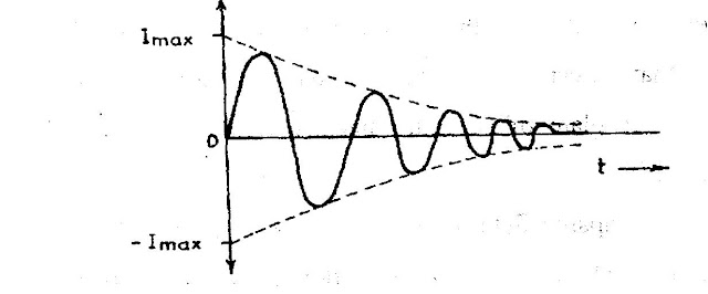
  •      The result is that the amplitude of oscillating current decreases gradually and eventually it becomes zero when all the energy is consumed as losses.
  •     Therefore, the tank circuit by itself will produce damped oscillations as shown below.


STABILIZATION OF AMPLITUDE:


  •     In all the oscillators the output waveform tends to be the maximum possible output that the amplifier can produce.
  •     Having large amplitudes will distort the output amplitude since the output amplitude is limited only by the amplifier output range.
  •     To minimize distortion and reduce the amplitude of the output waveform to an acceptable level amplitude stabilization circuitry must be employed.
  •     Amplitude stabilization operates by ensuring that oscillation ceases as the amplifier output approaches a predetermined level.
  •     As the output falls to an acceptable level the circuit continues to oscillate. For phase shift oscillators the amplifier gain should always exceed 29 to sustain oscillations.

Negative Resistance oscillator


  • When the operating point enters the region of positive resistance, the amplitude of oscillation is limited. 

  • To obtain the maximum output, the quiescent point must be accurately located at the center of the negative resistance region.The frequency of oscillation is given by,
                                                F = 1/2 root LC
  •  A tunnel diode has a characteristic with a negative resistance region between voltages of approximately 0.1 and 0.3 V and can be used as an oscillator at frequencies up to 100 0Hz.

 BARKHAUSEN CRITERION:

  •     The essential condition for maintaining oscillations are:

  •     | βA | = 1, i.e. the magnitude of loop gain must be unity.

  •     The total phase shift around the closed loop is zero or 360 degrees.

PRACTICAL CONSIDERATIONS:
  •     The condition that  | βA | = 1 gives a single and precise value of Aβ which should be set through out the operation of the oscillator circuit.
  •     But in practice, as transistor characteristics and performance of other circuit components change with time, | βA |  will become greater or less than unity.
  •  Hence, in all practical circuits | βA |  should be set greater than unity so that the amplitude of oscillation will continue to increase without limit but such an increase in amplitude is limited by the onset of the nonlinearity of operation in the active devices associated with the amplifier is shown below.

  •  In this circuit, Βa is larger than unity for positive feedback. This onset of Non linearity is an essential feature of all practical oscillators.

CONSTRUCTION OF N-CHANNEL JFET:


It consists of


Source (S):It is the terminal through which the majority charge carriers enter the

bar. The source current is denoted by IS.

Drain: It is the terminal through which the majority charge carriers leave the bar.

The current entering the drain D is ID .VDS is the drain source voltage.


Gate: Heavily doped P-type silicon is diffused on both sides of the N-type silicon bar

by which PN junctions are formed. These layers are joined together and called

gate G.

Channel: The region BC of the N-type bar in the depletion region is called

the channel. When VDS is applied between the source and the drain, majority

Carriers move from source to drain.


Heat Sinks Used In Power Transistors

  • Heat sinks are used for power transistors as the power dissipated at their collector junction is large. If heat dissipation is not done, this will cause large increases in junction temperature.


  • In a transistor, the collector to base junction temperature (temperature of surrounding air) rises or because of self-heating. The self-heating is due to the power dissipated at collector junction


  • This power dissipation at junction causes the junction temperature to rise, and this in turn increases the collector current which causes further increase in power dissipation. If the phenomenon continues then it may result in permanent damage of the transistor. This is known as thermal runaway.


  • In power transistor or large signal transistors, the power to be dissipated at the collector causes junction temperature to rise to a high level.


  • It is possible to increase the power handling capacity of the transistor if a device that can cause rapid conduction of heat away from the junction is used. Such a device is called a heat sink.


  • A heat sink is a mechanical device. It is connected to the case of the semiconductor device. So it is providing a path for the heat transfer.


  • The heat flows through the heat sink and is radiated to surrounding air. If a heat sink is not used then all the heat has to he transferred from a transistor case to surrounding air causing case temperature to increase.


  • If the power handled by the transistor is higher, then the case temperature will he higher. The temperature of the two types of power transistor is

                       Germanium: 100°C to 110°C


                       Silicon : 150°C to 200°C


  • Heat sinks increase the power rating (ie. power handling capacity) of a transistor by getting rid of the heat developed quickly.


  • It is in the form of a sheet of metal. Since the power dissipation within a transistor is mainly due to power dissipated at collector junction, the collector (connected to the case of the transistor) is bolted on to metal sheet for faster radiation of heat.


  • In this case, to prevent the collector from shorting to metal sheet, a thin mica washer is used between the two.


  • Fig shows a heat sink. The heat now radiate more quickly because of in creased surface area.


  • Sometimes the transistor is connected to a large heat sink with fins causing more efficient removal of heat from the transistor.


  • When heat flows out of a transistor, it passes through the case transistor and into the heat sink, which then radiates the heat into the surrounding air.


  • The temperature of the transistor case T will be slightly higher than the temperature of the heat sink which in turn is slightly higher than the ambient temperature TA.

  • Ambient Temperature: The heat produced at the junction passed through the transistor case (metal or plastic housing) are radiates to the surrounding air. The temperature of this air is known as the ambient temperature.

TRANSISTOR POWER RATING

  • Power transistors develop considerable amount of current and this current through the transistor elements themselves, as well as the internal connecting wires will generate a certain amount of heat.


  • This raises the temperature of collector junction and places a limit on the allowable power dissipation P Depending on the transistor type, a junction temperature in the range of 150° to 200°C will destroy the transistor.


  • Data sheets specify these junction temperature as Hence it becomes important with power transistors to bring out this heat at collector junction as quickly as possible and then conduct away from the unit as efficiency as possible.

SALIENT FEATURES OF POWER TRANSISTORS

  • The power capability of a transistor is limited by three major factors First, there is a maximum reverse voltage that the collector can withstand.


  • As the reverse voltage applied to co]lector base junction is increased beyond certain limit, the transistor gets damaged either due to

                                                1.Avalanche effect (or)

                                                2.Punch through effect


  • The second factor that limits the maximum power capability of transistor is the decrease in current gain with increased current.


  • The third factor that establishes a limit to the maximum power output of a transistor is the safe amount of heat that the material or junction can withstand.


  • Another way of stating this is maximum power dissipation of the transistor.


  • Another important factor be considered in power transistors is its frequency response because of power gain that falls off rapidly (above certain point).


  • An important characteristic in establishing the frequency behaviour of a transistor is the time required for a signal to travel from emitter to collector. This, in-turn, depends upon the mobility of the carriers within the silicon.


  • It is not possible to apply signals whose frequency changes are very rapid. Because the carriers are unable to transport the charges from emitter to collector at these rapid change of frequency.


  • Electrons move almost twice as fast as holes and hence NPN transistors have higher frequency response than PNP transistors.


  • Another factor that limits the high frequency response is the capacitance between section of a transistor.


  • The higher the frequency, the lower the impedance of the shunting capacitor and greater its shunting effect on the applied signal.

Power transistors are classified depending upon:


        1.Capability of dissipating power

        2.Current carrying capacity 

        3.Frequency of operation


  • Transistors which can dissipate power in the range of 1 to 10 watts are classified as lower transistors.


  • A medium power transistor is one which can dissipate power in the range of 10 watts to 100 watts.


  • High power transistors are transistors that can dissipate above 100 watts.

Depending upon continues current carrying capacity transistors are classified as

1.Low current transistors

                   Those which can carry current less than 3 amperes continuously

2.Medium current transistors

               Those capable of carrying currents from 3 amperes to 10 amperes.

3.High current transistors

                   Those capable of handling current exceeding 10 amperes.


  • Silicon power transistors having voltage rating less than 60 volts are called low- voltage type. Medium voltage transistors have voltage rating from 90 to 300 volts.


  • Beyond this range comes high voltage transistor.


  • Low frequency transistors are those which operate below 3K Transistors which can operate in the frequency of 3 to 15 KHz are middle frequency transistors and transistors capable of operating at higher frequencies efficiently are high frequency type.

POWER TRANSISTOR

  • Power amplifiers are used to provide power required to drive an current operated load.

  • This load maybe loud speaker in an audio circuit, a horizontal deflection yoke in a video circuit, a magnetic core in a computer memory circuit or a servo motor in an industrial control circuit.

  • These amplifiers operate with large input signals. In a power amplifier, the increased power must come from the D.C power source supplying the active device used in the circuit. Power transistors are used an active devices.

  • Active device in power amplifier, circuit is to reproduce in the output circuit a large power signal that is a replica of the relatively small signal applied to its input circuit, differing only in the amplitude of power

  • Power amplifier circuits are used in both A.F. and R.F. circuits.

  • In power amplifier circuits, the active devices may be operated as class A, class All, class B or class C. Although all classes of operation may he used in both R.F. and AT. Power amplifier circuits. Class C is used primarily in R.F. amplifiers, due to its higher efficiency

  • Depending upon amount of power output required, the active devices used in power amplifiers may be operated as (1) in single (2) in parallel (3) in push pull.

Black box theory


  • Transistor is  shown  as  a four terminal  black  box  in  Fig.  There  are two input terminals A and B and two output terminals C and D.

  • The voltage at the input terminal is V1and input current is I1 and those at the output terminals are V2 and I2.

  • The  signals  V1  and  I1,  V2  and  I2  are  shown  with  their  conventional  positive polarities.
                                                           Block diagram of black box

  • In  general  two  equations  are  formed  using  these  four  signal  quantities  and the circuit parameters of the transistor.

  • The circuit parameters are defined based on the selection of signal quantities in the left side and right side of the equations.

  • Six sets of parameters are used for transistor circuit analysis. Out of them the following three are commonly used.
1.Impedance or Z-parameters

2.Admittance or Y-parameters

3.Hybrid or h-parameters

Among these h’ parameters are the most useful for transistor circuit analysis due to the following reasons.

1.h-parameters form a combination of impedance and admittance parameters.

2.h-parameters are easiest to measure.

3.h-parameters almost correspond to the actual operating conditions.

4.h-parameters  produce  more accurate  results  in  the  analysis  of  amplifiercircuits.

COMMON COLLECTOR CONFIGURATION OF A TRANSISTOR


COMMON COLLECTOR CONNECTION

In  this  configuration  the  input  is  applied  between the  base  and  the  collector and  the  output  is  taken  from  the  collector  and  the  emitter.  Here  the  collector  is common to both the input and the output circuits as shown in Fig.

                                                       Common Collector Transistor Circuit

In  common  collector  configuration  the  input  current  is  the  base current  IB  and  the output current is the emitter current IE. The ratio of change in emitter current to the  change in the base current is called current amplification factor.

It is represented by 


COMMON COLLECTOR CIRCUIT

A test  circuit  for determining the  static characteristic  of an NPN transistor is shown in Fig. In this circuit the collector is common to both the input and the output circuits.   To   measure   the   base   and   the   emitter   currents,   milli   ammeters   are connected in series with the base and the emitter circuits. Voltmeters are connected   across the input and the output circuits to measure VCE and VCB

INPUT CHARACTERISTICS

                                                Common Collector Input Characteristic Curve


  • It  is  a  curve  which  shows the  relationship  between the  base  current,  IB and the collector base voltage VCB at constant VCE This method of determining the characteristic is as follows.

  • First, a suitable voltage is applied between the emitter and the collector. Nextthe  input  voltage  VCB  is  increased  in  a  number  of  steps  and  corresponding values of IE are noted.

  • The base current is taken on the y-axis, and the input voltage is taken on the x-axis. Fig. shows the family of the input characteristic at different collector- emitter voltages.

  • The following points may be noted from the family of characteristic curves.  1.Its  characteristic  is  quite  different  from  those  of  common  base  andcommon emitter circuits.
2.When VCB increases, IB is decreased.

Output Characteristics

  • It is a curve which shows the relationship between the emitter current l and collector-emitter voltage, the method of determining the output characteristic is as follows.

  • First,  by  adjusting  the  input  a  suitable  current  IB  is  maintained.  Next  VCB increased in a number of steps from zero and corresponding values of IE are  noted.

  • The above whole procedure is repeated for different values of IB. The emitter current  is  taken  on  the  Y-axis  and  the  collector-emitter  voltage is  taken  on the X-axis.

  • Fig shows the family of output characteristics at different base current values. The following points are noted from the family of characteristic curves.
                                         Common Collector Output Characteristic Curves

1.This  characteristic  is  practically  identical  to  that   of  the  common  emitter circuit.

2.Its current gain characteristic for different values of VCE is also similar to that of a common emitter circuit.

COMMON EMITTER CONFIGURATION OF A TRANSISTOR


COMMON EMITTER CONNECTION


In this configuration, the input is applied between the base and the emitter and the output is taken from the collector and the emitter. In this connection, the emitter is common to both the input and the output circuits as shown in Fig. In the common emitter configuration the input current is the base current IB and the output current is the collector current IC. The ratio of change in collector current to the change in base current at constant collector-emitter voltage is called base current amplification factor ( ).


COMMON EMITTER CIRCUIT

A test circuit for determining the static characteristic of an NPN transistor is shown in Fig In this circuit emitter is common to both input and output circuits. To measure the base and collector current milli ammeters are connected in series with the base and the output circuits. Voltmeters are connected across the input and the output circuits to measure VBE and VCE There are two potentiometers R1 and R2 to vary the supply voltages VCC and VBB.

              Circuit arrangement to determine static characteristic of common emitter


Input Characteristics

It is a curve which shows the relationship between base current IB and the emitter-base voltage, VBE at constant VCE. The method of determining the characteristic is as follows.


                                                Common emitter input characteristic curve


First, by means of R1 suitable voltage is applied from VCC, Next, voltage VBE is increased in number of steps and corresponding values of IB are noted. The base current is taken on the Y-axis and the base-emitter voltage is taken on the X-axis.

Fig shows the input characteristic for common emitter configuration. The following points may be noted from the characteristic.

1. The input resistance of the transistor is equal to the reciprocal of the slope of the input characteristic curve.


2. The initial portion of the curve is not linear.

3. The input resistance varies considerable from a value 4 kilo ohm to a value of 600 ohms.

4. In the case of silicon transistor the curves break away from zero current for voltage in the range of 0.5 to  0.6 volt whereas for germanium transistor the break away point is in the range 0.1 to 0.2V


Output Characteristics

It is a curve which shows the relationship between the collector IC and the collector- emitter voltage VCE. This method of determining the characteristic is as follows.

First by means of R1 a suitable base current IB is maintained. Next VCE is increased from zero, in a number of steps and corresponding values of IC are noted. The above whole procedure isrepeated for different values of IB. The collector current is taken on the Y-axis. Fig shows the family of output characteristics at different base current values. The following points may be noted from the family of characteristic curves.


                                      Common emitter characteristic curve


1.The collector current IC increases rapidly to a saturation level for fixed value of IB. But at the same time VCE increases from zero.

2.A small amount of collector current flows even when IB=0 the current is called ICEO. Now main collector current is zero and the transistor is cut-off.

3.The output characteristics may be divided into three regions.


  • The active region


  • Cut-off region


  • Saturation region

Active region: In this region the collector is reverse biased and the emitter is forward biased. The collector current, IC response is most sensitive for changes in IB. Since = /(1- ) and also is very close to unity. (I - ) is very small. Therefore, a slight change in a produces very large change in b and so the collector current,


is changed substantially

Cut-off region: When IE= 0 and IC = ICO, the cut-off condition of the transistor is reached. It is necessary that emitter junction has to reverse biased slightly i.e., 0.1 V for germanium and 0 volt for silicon.

In this region

Saturation region: In this region incremental change, in IB do not produce corresponding large changes in IC. The region is also refer to as bottomed region because the voltage has fallen near the bottom of the characteristic. In this configuration saturation is entered while collector is still reverse biased.


Labels

PROJECTS 8086 PIN CONFIGURATION 80X86 PROCESSORS TRANSDUCERS 8086 – ARCHITECTURE Hall-Effect Transducers INTEL 8085 OPTICAL MATERIALS BIPOLAR TRANSISTORS INTEL 8255 Optoelectronic Devices Thermistors thevenin's theorem MAXIMUM MODE CONFIGURATION OF 8086 SYSTEM ASSEMBLY LANGUAGE PROGRAMME OF 80X86 PROCESSORS POWER PLANT ENGINEERING PRIME MOVERS 8279 with 8085 MINIMUM MODE CONFIGURATION OF 8086 SYSTEM MISCELLANEOUS DEVICES MODERN ENGINEERING MATERIALS 8085 Processor- Q and A-1 BASIC CONCEPTS OF FLUID MECHANICS OSCILLATORS 8085 Processor- Q and A-2 Features of 8086 PUMPS AND TURBINES 8031/8051 MICROCONTROLLER Chemfet Transducers DIODES FIRST LAW OF THERMODYNAMICS METHOD OF STATEMENTS 8279 with 8086 HIGH VOLTAGE ENGINEERING OVERVOLATGES AND INSULATION COORDINATION Thermocouples 8251A to 8086 ARCHITECTURE OF 8031/8051 Angle-Beam Transducers DATA TRANSFER INSTRUCTIONS IN 8051/8031 INSTRUCTION SET FOR 8051/8031 INTEL 8279 KEYBOARD AND DISPLAY INTERFACES USING 8279 LOGICAL INSTRUCTIONS FOR 8051/8031 Photonic Transducers TECHNOLOGICAL TIPS THREE POINT STARTER 8257 with 8085 ARITHMETIC INSTRUCTIONS IN 8051/8031 LIGHTNING PHENOMENA Photoelectric Detectors Physical Strain Gage Transducers 8259 PROCESSOR APPLICATIONS OF HALL EFFECT BRANCHING INSTRUCTIONS FOR 8051/8031 CPU OF 8031/8051 Capacitive Transducers DECODER Electromagnetic Transducer Hall voltage INTEL 8051 MICROCONTROLLER INTEL 8251A Insulation Resistance Test PINS AND SIGNALS OF 8031/8051 Physical Transducers Resistive Transducer STARTERS Thermocouple Vacuum Gages USART-INTEL 8251A APPLICATIONs OF 8085 MICROPROCESSOR CAPACITANCE Data Transfer Instructions In 8086 Processors EARTH FAULT RELAY ELECTRIC MOTORS ELECTRICAL AND ELECTRONIC INSTRUMENTS ELECTRICAL BREAKDOWN IN GASES FIELD EFFECT TRANSISTOR (FET) INTEL 8257 IONIZATION AND DECAY PROCESSES Inductive Transducers Microprocessor and Microcontroller OVER CURRENT RELAY OVER CURRENT RELAY TESTING METHODS PhotoConductive Detectors PhotoVoltaic Detectors Registers Of 8051/8031 Microcontroller Testing Methods ADC INTERFACE AMPLIFIERS APPLICATIONS OF 8259 EARTH ELECTRODE RESISTANCE MEASUREMENT TESTING METHODS EARTH FAULT RELAY TESTING METHODS Electricity Ferrodynamic Wattmeter Fiber-Optic Transducers IC TESTER IC TESTER part-2 INTERRUPTS Intravascular imaging transducer LIGHTNING ARRESTERS MEASUREMENT SYSTEM Mechanical imaging transducers Mesh Current-2 Millman's Theorem NEGATIVE FEEDBACK Norton's Polarity Test Potentiometric transducers Ratio Test SERIAL DATA COMMUNICATION SFR OF 8051/8031 SOLIDS AND LIQUIDS Speed Control System 8085 Stepper Motor Control System Winding Resistance Test 20 MVA 6-digits 6-digits 7-segment LEDs 7-segment A-to-D A/D ADC ADVANTAGES OF CORONA ALTERNATOR BY POTIER & ASA METHOD ANALOG TO DIGITAL CONVERTER AUXILIARY TRANSFORMER AUXILIARY TRANSFORMER TESTING AUXILIARY TRANSFORMER TESTING METHODS Analog Devices A–D BERNOULLI’S PRINCIPLE BUS BAR BUS BAR TESTING Basic measuring circuits Bernoulli's Equation Bit Manipulation Instruction Buchholz relay test CORONA POWER LOSS CURRENT TRANSFORMER CURRENT TRANSFORMER TESTING Contact resistance test Current to voltage converter DAC INTERFACE DESCRIBE MULTIPLY-EXCITED Digital Storage Oscilloscope Display Driver Circuit E PROMER ELPLUS NT-111 EPROM AND STATIC RAM EXCITED MAGNETIC FIELD Electrical Machines II- Exp NO.1 Energy Meters FACTORS AFFECTING CORONA FLIP FLOPS Fluid Dynamics and Bernoulli's Equation Fluorescence Chemical Transducers Foil Strain Gages HALL EFFECT HIGH VOLTAGE ENGG HV test HYSTERESIS MOTOR Hall co-efficient Hall voltage and Hall Co-efficient High Voltage Insulator Coating Hot-wire anemometer How to Read a Capacitor? IC TESTER part-1 INSTRUMENT TRANSFORMERS Importance of Hall Effect Insulation resistance check Insulator Coating Knee point Test LEDs LEDs Display Driver LEDs Display Driver Circuit LM35 LOGIC CONTROLLER LPT LPT PORT LPT PORT EXPANDER LPT PORT LPT PORT EXTENDER Life Gone? MAGNETIC FIELD MAGNETIC FIELD SYSTEMS METHOD OF STATEMENT FOR TRANSFORMER STABILITY TEST METHODS OF REDUCING CORONA EFFECT MULTIPLY-EXCITED MULTIPLY-EXCITED MAGNETIC FIELD SYSTEMS Mesh Current Mesh Current-1 Moving Iron Instruments Multiplexing Network Theorems Node Voltage Method On-No Load And On Load Condition PLC PORT EXTENDER POTIER & ASA METHOD POWER TRANSFORMER POWER TRANSFORMER TESTING POWER TRANSFORMER TESTING METHODS PROGRAMMABLE LOGIC PROGRAMMABLE LOGIC CONTROLLER Parallel Port EXPANDER Paschen's law Piezoelectric Wave-Propagation Transducers Potential Transformer RADIO INTERFERENCE RECTIFIERS REGULATION OF ALTERNATOR REGULATION OF THREE PHASE ALTERNATOR Read a Capacitor SINGLY-EXCITED SOLIDS AND LIQUIDS Classical gas laws Secondary effects Semiconductor strain gages Speaker Driver Strain Gages Streamer theory Superposition Superposition theorem Swinburne’s Test TMOD TRANSFORMER TESTING METHODS Tape Recorder Three-Phase Wattmeter Transformer Tap Changer Transformer Testing Vector group test Virus Activity Voltage Insulator Coating Voltage To Frequency Converter Voltage to current converter What is analog-to-digital conversion Windows work for Nokia capacitor labels excitation current test magnetic balance voltage to frequency converter wiki electronic frequency converter testing voltage with a multimeter 50 hz voltages voltmeter

Search More Posts

Followers