Showing posts with label 8085 Processor- Q and A-2. Show all posts

SERIAL DATA COMMUNICATION IN 8051 MICROCONTROLLER

•    The fastest way of transmitting data, within a microcomputer is parallel data transfer.

•    For transferring data over long distances, however, parallel data transmission requires too many wires.

•    For long distance transmission, data is usually converted from parallel form to serial form so that it can be sent on a single wire or pair of wires.

•    Serial data received from a distant source is converted to parallel form and it can be easily transferred on the microcomputer buses.

•    The types of communication systems are,

1.    Simplex   2.  Half-duplex    3.  Full-duplex
  •    In simplex communication, data can be transmitted only in one direction, ie. data from sensors to processor. Eg : commercial radio stations.
  •     In half-duplex transmission, data can be transmitted in either direction between two systems, but can occur only in one direction at a time. Eg : two-way radio system, where one user always listens while the other talks because the receiver circuitry is turned off during transmit.
  •   In full duplex, the data can be send and received at the same time. Eg : A normal phone conversation.

·         Serial data can be sent by two ways.
They are,
1.      Synchronous communication    
  
2.      2. Asynchronous communication

  In synchronous transmission, data are transmitted in block at a constant rate.

  The start and end of a block are identified with specific bytes or bit patterns.

  In asynchronous transmission, data is transmitted one by one.

  The beginning of a data character is indicated by the line going low for 1 bit time. This bit is called a start bit.

  The data bits are then sent out on the line one after the other. Note that the least-significant bit is sent out first. Depending on the system, the data word may consist of 5, 6, 7 or 8 bits.

 Following the data bits is a parity bit, which is used to check for errors in received data.

The line is returned high for at least 1-bit time to identify the end of the character. This always-high bit is referred to as a stop bit. Some systems may use 2 stop bits.


    The bit format for asynchronous data transmission is,


•    The term baud rate is used to indicate the rate at which serial data is being transferred.
Baud rate = 1/ time for a bit cell

•    A device such as INTEL 8251A, which can be programmed to do either asynchronous or synchronous communication, is often called USART (Universal Synchronous Asynchronous Receiver Transmitter).

•    A device such as the National 1NS8250, which can only do asynchronous communication, is often referred to as a Universal Asynchronous Receiver Transmitter (UART).

•    For sending serial data over long distances the standard telephone system is a convenient path, because the wiring and connections are already in place.

•    Standard phone lines often referred to as switched lines because any two points can be connected together through a series of switches and have a bandwidth of about 300 to 3000 Hz.

•    But digital signals require very large bandwidth (typically 5 MHz). Therefore, digital signals cannot be sent directly over standard phone lines. So, the digital signals are converted to audio-frequency tones, which are in the frequency range.

•    The device used to do this conversion and to convert transmitted tones back to digital information is called a MODEM.

•    Modems and other equipment used to send serial data over long distances are known as data communication equipment or DCE. The terminals and computers that are sending or receiving the serial data are referred to as data terminal equipment or DTE.

 RS-232C serial data standard:

•    In serial I/O, data can be transmitted as either current or voltage.

•    When data are transmitted as voltage, the commonly used standard is known as RS-232C.

•    This standard, proposes a maximum of 25 signals for the bus used for serial data transfer.

•    The 25 signals of RS-232C are,


•    In practice the first 9-signals are sufficient for most of the serial data transmission scheme and so the RS-232C bus signals are terminated on a D-type 9-pin connector.


•    When all the 25 signals are used, then RS-232C serial bus is terminated on a 25-pin connector.


•    The RS-232C signal levels are not compatible with TTL logic levels. Hence for interfacing TTL devices, level converters or RS-232C line drivers are employed.

•    The popularly used level converters are,

1.    MC1488 - TTL to RS-232C level converter.

2.    MC1489 - RS-232C to TTL level converter.

3.    MAX 232 - Bidirectional level converter.

(Max 232 is equivalent to a combination of MC 1488 and MCI 489 in single IC)

•    The pin diagram of MAX 232 is,


•    For MAX 232 all capacitor should be 1µF.

•    The voltage rating of all capacitor should above 10V.

ADDRESSING MODES OF 8051/8031 MICROCONTROLLER

--> •    Every instruction of a program has to operate on a data.

•    The method of specifying the data to be operated by the instruction is called addressing.

•    The 8031 has the following types of addressing.

1.    Immediate Addressing

2.    Direct Addressing

3.    Register Addressing

4.    Register Indirect Addressing

5.    Implied Addressing


6.    Relative Addressing

1. IMMEDIATE ADDRESSING :

In immediate addressing mode, an 8/16 bit immediate data / constant is specified in the instruction itself.

MOV A, #6CH  :- Move the immediate data 6CH given in the instruction to A-register.

MOV DPTR, #0100H   :- Load the immediate 16-bit constant given in the instruction in DPTR (Data pointer). This constant will be an address of data memory location.


2. DIRECT ADDRESSING    :

In direct addressing mode, the address of the data is directly specified in the instruction.
The direct address can be the address of an internal data RAM location (00H to 7FH) or address of special function register (80H to FFH).

MOV A, 07 H  :- The address of R7 register of bank-0 is 07. This instruction will move the content of R7 register to A-register (Accumulator).

3.REGISTER ADDRESSING :

In register addressing mode, the instruction will specify the name of register in which data available.

MOV R2,A   :- The content of A-register (accumulator) is moved to register R2.


4. REGISTER INDIRECT ADDRESSING :

In this mode, the instruction specifies the name of the register in which the address of the data is available. The internal data RAM locations (00H to 7FH) can be addressed indirectly through registers R1 and R0. The external RAM can be addressed indirectly through DPTR.

MOV A, @R0  :- The internal RAM Location R0 holds the address of data. The content of RAM location addressed by R0 is moved to A-register (Accumulator).

5. IMPLIED ADDRESSING :

In implied addressing mode, the instruction itself specifies the data to be operated by the instruction.
CPL C   :- Complement carry flag.


6. RELATIVE ADDRESSING:

In relative addressing mode, the instruction specifies the address relative to program counter.
The instruction will carry an offset whose range is -l2810 to +l2710 .
The offset is added to PC to generate 16-bit physical address.

JC Offset :- If carry is one then the program control jump to an address obtained by adding the content of program counter and offset value in the instruction.

FEATURES & FUNCTIONAL BLOCK DIAGRAM OF 8259 PROCESSOR

1. It is programmed to work with either 8085 or 8086 processor. 

2. It manage 8-interrupts according to the instructions written into its control registers.

3.  In  8086  processor,  it  supplies  the  type  number  of  the  interrupt  and  the  type  number  is programmable.  In  8085  processor,  the  interrupt  vector  address  is  programmable.  The priorities of the interrupts are programmable.

4. The interrupts can be masked or unmasked individually.

5. The 8259s can be cascaded to accept a maximum of 64 interrupts.

FUNCTIONAL BLOCK DIAGRAM OF 8259:

•    It has eight functional blocks. They are,

1.   Control logic

2.   Read Write logic

3.   Data bus buffer

4.   Interrupt Request Register (IRR)

5.   In-Service Register (ISR)

6.   Interrupt Mask Register (IMR)

7.   Priority Resolver (PR)

8.   Cascade buffer.

The data bus and its buffer are used for the following activities.

1.   The processor sends control word to data bus buffer through D0-D7.

2.   The processor read status word from data bus buffer through D0-D7.

3.  From the  data  bus  buffer  the  8259  send  type  number  (in  case  of  8086)  or  the  call opcode and    address (in case of 8085) through D0-D7 to the processor.


•    The processor uses the RD (low), WR (low) and A0 to read or write 8259.

•    The 8259 is selected by CS (low).

•    The  IRR  has  eight  input  lines  (IR0-IR7)  for  interrupts.  When  these  lines  go  high,  the request is stored in IRR. It registers a request only if the interrupt is unmasked.

•    Normally  IR0  has  highest  priority  and  IR7  has  the  lowest  priority.  The  priorities  of  the interrupt request input are also programmable.

•    First  the  8259  should  be  programmed  by  sending  Initialization  Command  Word  (ICW)
and Operational Command Word (OCW). These command words will inform 8259 about the following,

* Type of interrupt signal (Level triggered / Edge triggered).
* Type of processor (8085/8086).
* Call address and its interval (4 or 8)
* Masking of interrupts.
* Priority of interrupts.
* Type of end of interrupts.


•    The  interrupt  mask  register  (IMR)  stores  the  masking  bits  of  the  interrupt  lines  to  be masked. The relevant information is send by the processor through OCW.

•    The in-service register keeps track of which interrupt is currently being serviced.

•    The  priority  resolver  examines  the  interrupt  request,  mask  and  in-service  registers  and determines whether INT signal should be sent to the processor or not.

•    The cascade buffer/comparator is used to expand the interrupts of 8259.

•    In cascade connection one 8259 will be directly interrupting 8086 and it is called master
8259.

•    To  each  interrupt  request  input  of  master  8259  (IR0-IR7),  one  slave  8259  can  be connected. The 8259s interrupting the master 8259 are called slave 8259s.

•    Each 8259 has its own addresses so that each 8259 can be programmed independently by sending command words and independently the status bytes can be read from it.

•    The  cascade  pins  (CAS0,  CAS1   and  CAS2)  from  the  master  are  connected  to  the corresponding pins of the slave.

•    For the slave 8259, the SP (low) / EN (low) pin is tied low to let the device know that it is
a slave.

•    The SP (low) / EN (low) pin can be used as input or output signal.

•    In non-buffered mode it is used as input signal and tied to logic-I in master 8259 and logic-0 in slave 8259.

•    In buffered mode it  is used as output signal to disable the data buffers while data is transferred from 8259A to the CPU.

Cascade Connection of 8059


PROGRAMMABLE DMA CONTROLLER - INTEL 8257:

•    It is a device to transfer the data directly between IO device and memory without through
the CPU. So it performs a high-speed data transfer between memory and I/O device.
•    The features of 8257 is,

1.   The 8257 has four channels and so it can be used to provide DMA to four I/O
devices
2.   Each channel can be independently programmable to transfer up to 64kb of data
by DMA.
3.   Each  channel  can  be  independently  perform  read  transfer,  write  transfer  and verify transfer.

•    It is a 40 pin IC and the pin diagram is,


Functional Block Diagram of 8257:

•    The functional block diagram of 8257 is shown in fig.
•    The  functional  blocks  of  8257  are  data  bus  buffer,  read/write  logic,  control  logic, priority resolver and four numbers of DMA channels.
•    Each  channel  has  two  programmable  16-bit  registers  named  as  address  register  and count register.


•    Address register is used to store the starting address of memory location for DMA data transfer.
•    The    address    in    the    address    register    is    automatically    incremented    after    every read/write/verify transfer.
•    The count register is used to count the number of byte or word transferred by DMA
•    The format of count register is,


•    14-bits B0-B13  is used to  count value and  a 2-bits is used for indicate the type of DMA
transfer (Read/Write/Veri1 transfer).
•    In read transfer the data is transferred from memory to I/O device.
•    In write transfer the data is transferred from I/O device to memory.
•    Verification   operations   generate   the   DMA   addresses   without   generating   the   DMA
memory and I/O control signals.
•    The 8257 has two eight bit registers called mode set register and status register.
•    The format of mode set register is,


•    The use of mode set register is,

1.   Enable/disable a channel.
2.   Fixed/rotating priority
3.   Stop DMA on terminal count.
4.   Extended/normal write time.
5.   Auto reloading of channel-2.


•    The bits B0, B1, B2, and B3 of mode set register are used to enable/disable channel -0, 1, 2
and 3 respectively. A one in these bit position will enable a particular channel and a zero
will disable it
•    If the bit B4 is set to one, then the channels will have rotating priority and if it zero then the channels wilt have fixed priority.
  1.  In rotating priority after servicing a channel its priority is made as lowest.
  2.  In fixed priority the channel-0 has highest priority and channel-2 has lowest priority.

•    If the bit B5  is set to one, then the timing of low write signals (MEMW and IOW) will be extended.
•    If the bit B6 is set to one then the DMA operation is stopped at the terminal count.
•    The bit B7 is used to select the auto load feature for DMA channel-2.
•    When bit B7  is set to one, then the content of channel-3 count and address registers are loaded  in  channel-2  count  and  address  registers  respectively  whenever  the  channel-2
reaches terminal count. When this mode is activated the number of channels available for
DMA reduces from four to three.
•    The format of status register of 8257 is shown in fig.


•    The  bit  B0,  B1,  B2,  and  B3  of  status  register  indicates  the  terminal  count  status  of channel-0, 1,2 and 3 respectively. A one in these bit positions indicates that the particular
channel has reached terminal count.
•    These status bits are cleared after a read operation by microprocessor.
•    The bit B4  of status register is called update flag and a one in this bit position indicates that  the  channel-2  register  has  been  reloaded  from  channel-3  registers  in  the  auto  load mode of operation.
•    The internal addresses of the registers of 8257 are listed in table.


INTEL 8279 MICROPROCESSOR - KEYBOARD/DISPLAY CONTROLLER

The INTEL 8279 is specially developed for interfacing keyboard and display devices
to 8085/8086/8088 microprocessor based system. The important features of 8279 are,

• Simultaneous keyboard and display operations.
• Scanned keyboard mode.
• Scanned sensor mode.
• 8-character keyboard FIFO.
• 1 6-character display.
• Right or left entry 1 6-byte display RAM.
• Programmable scan timing.

Block diagram of 8279:

•    The functional block diagram of 8279 is shown.


•    The four major sections of 8279 are keyboard, scan, display and CPU interface.

Keyboard section:

•    The keyboard section consists of eight return lines RL0 – RL7 that can be used to form the columns of a keyboard matrix.

•    It   has   two   additional   input   :   shift   and   control/strobe.   The   keys   are   automatically debounced.

•    The two operating modes of keyboard section are 2-key lockout and N-key rollover.

•    In the 2-key lockout mode, if two keys are pressed simultaneously, only the first key is recognized.

•    In the N-key rollover mode simultaneous keys are recognized and their codes are stored in
FIFO.

•    The keyboard section also have an 8 x 8 FIFO (First In First Out) RAM.

•    The FIFO can store eight key codes in the scan keyboard mode. The status of the shift key and control key are also stored along with key code. The 8279 generate an interrupt signal when there is an entry in FIFO. The format of key code entry in FIFO for scan keyboard mode is,


•    In sensor  matrix mode the condition (i.e., open/close status) of 64  switches is stored in FIFO RAM. If the condition of any of the switches changes then the 8279 asserts IRQ as high to interrupt the processor.

Display section:

•    The display section has eight output lines divided into two groups A0-A3 and B0-B3.

•    The output lines can be used either as a single group of eight lines or as two  groups of four lines, in conjunction with the scan lines for a multiplexed display.

•    The output lines are connected to the anodes through driver transistor in case of common cathode 7-segment LEDs.

•    The cathodes are connected to scan lines through driver transistors.

•    The display can be blanked by BD (low) line.

•    The display section consists of 16 x 8 display RAM. The CPU can read from or write into any location of the display RAM.

Scan section:


•    The scan section has a scan counter and four scan lines, SL0 to SL3.

•    In decoded scan mode, the output of scan lines will be similar to a 2-to-4 decoder.

•    In encoded scan mode, the output of scan lines will be binary count, and so an external decoder should be used to convert the binary count to decoded output.

•    The scan lines are common for keyboard and display.

•    The scan lines are used to form the rows of a matrix keyboard and also connected to digit drivers of a multiplexed display, to turn ON/OFF.

CPU interface section:

•    The CPU interface section takes care of data transfer between 8279 and the processor.

•    This section has eight bidirectional data lines DB0  to DB7  for data transfer between 8279
and CPU.

•    It  requires  two  internal  address  A  =0  for  selecting  data  buffer  and  A  =  1  for  selecting control register of8279.

•    The control signals WR (low), RD (low), CS (low) and A0 are used for read/write to 8279.

•    It has an interrupt request line IRQ, for interrupt driven data transfer with processor.

•    The  8279  require  an  internal  clock  frequency  of  100  kHz.  This  can  be  obtained  by dividing the input clock by an internal prescaler.

•    The RESET signal sets the 8279 in 16-character display with two -key lockout keyboard modes.

Programming the 8279:

•    The  8279  can  be  programmed  to  perform  various  functions  through  eight  command words.

INTEL 8255 Programmable Peripheral Interface (PART-2)

Internal block diagram of 8255

The ports are grouped as Group A and Group B. The group A has port A, port C upper and its control circuit. The group B has port B, port C lower and its control circuit. The Read/Write control logic requires six control signals. These signals are given below.


RD (Read) :   This control signal enables the read operation.
                     When this signal is LOW, the microprocessor reads data from a selected I/O port of the 
                      8255A.

WR (Write):  This control signal enables the write operation.
                       When this signal goes LOW, the microprocessor writes into a selected I/O port
                       or the control register.

RESET:         This is an active HIGH signal.
                       It clears the control register and set all ports in the input mode.

CS, A0  and A1 : These are device select signals.
                             The CS is connected to the decoder in the system.
                             A0 and A1 are generally connected to A0 and A1 of the processor.

(Alternatively, A0 and A1 can be connected to any two-address lines of the processor).
8255 can be either Memory mapped or I/O mapped in the system.

A0 and A1 address lines can be made to select any one of the following four internal devices as shown on right side.


Programming 8255:
The 8255 has two control words, one for specifying 1/O functions and another for bit set/reset mode of port C. Both the control words are written in the same control register.

The control register differentiate them by the value of bit D7 .The bit set/reset control word does not affect the functions of ports A and B.

Bit D7 of the control register specifies either the 1/0 function or the bit set / reset function.
If bit D7 = 1, then the bits D6 – D0 determine 1/0 functions in various modes.
If bit D7 = 0, then the bits D6 – D0 determine the pin of port C to be set or reset.


The 8255 ports are programmed (or initialized) by writing a control word in the control register.

For setting 1/0 functions
and mode of operation the 1/0 mode control word is send to control register. The format of the 1/0 mode set control word is shown below.

For setting/resetting (BSR mode) a pin of port C, the bit set/ reset control word is sent to control register. The format of bit set/reset control word is shown below.


The data transfer between the processor and the port can be either interrupt driven or through status check.

In the interrupt driven data transfer scheme, when the port is ready, it interrupts the processor for a read or write operation.

In status check technique, the processor polls the status of the port and checks whether the port is ready for data transfer or not. The status of the ports A and B can be known by reading the port C. When the port is ready for data transfer, the processors executes a read or write cycle.

INTEL 8255 Programmable Peripheral Interface (PART-1)

Intel 8255 is a programmable peripheral interface chip designed for parallel communication between microprocessor and I/O devices, which have a speed mismatch between each other.


Features of 8255:

•It has three 8-bit ports
•It can be operated in three different modes in I/O mode and in BSR mode

IC 8255 has three ports A, Band C. The ports A and B are 8 bit parallel ports. Port A can be programmed to work in any one of the three modes as input or output port. The three operating modes are

Mode-0  - Simple I/O port
Mode-l   - Handshake I/O port
Mode-2  - Bidirectional I/O port.


The port B can be programmed to work either in mode-0 or mode-1. The port C pins (8-pins) have different assignments depending on the mode of port A and B. If port A and B are programmed in mode-0, then the port C can perform anyone of the following function.

1. As 8 bit parallel port in mode-0 for input or output.
2. As two numbers of 4 bit parallel port in mode-O for input or output.
3. The individual pins of port C can be set or reset for various control applications.

The various functions (assignments) of port C during the different operating modes of port A and B are listed in Table below.


If ports A and Bare programmed in mode-l or mode-2, then some of the pins of port C are used for handshake signals and the remaining pins can be used as input/output lines or individually set/reset for control applications.


I/0 Modes of 8255

Mode-0: In this mode, all the three ports can be programmed either as input or output port. In mode-O, the outputs are latched and the inputs are not latched. The ports do not have handshake or Interrupt capability. The ports in mode-o can be used to interface DIP switches, Hexa-keypad, LED's and 7-segment LED's to the processor.

Mode-l: In this mode, only ports A & B can be programmed either as input or output port. In mode-1, handshake signals are exchanged between the processor and peripherals prior to data transfer. The port C pins are used for  handshake signals. Input and output data are latched. Interrupt driven data transfer scheme is possible.

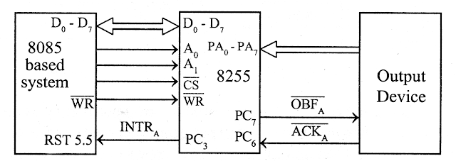
8255 Handshake Input port (Mode 1)


8255 Handshake Output port (Mode 1)\


Mode-2: In this mode, the port will be a bi-directional port (i.e., the processor can perform both read and write operations with an I/O device connected to a port in mode-2).
Only port-A can be programmed to work in mode-2. Five pins of port C are used for handshake signals. This mode is used primarily in applications such as data transfer between two computers or floppy disk controller interface.


Pins & Signals of 8255

The pin description of 8255 is shown in figure below. It has 40 pins and requires a single +5V supply.


INTEL 8085 Processor - Question & Answers (part-2)

In  a microprocessor system using  8085,  the  memory  requirement  is 8kb  EPROM  and 8kb  RAM.  For  interfacing  I/O  devices,  three  numbers  of  8255  are  required.  Select suitable memories and explain how they are interfaced to the system. Interface the 8255 by memory mapping.?

    The IC 2764 is selected for EPROM memory and the IC 6264 is selected for RAM memory.
    Both the memory lC have time compatibility with 8085 processor.
    The  8kb  EPROM,  2764  require  13  address  tines.  The  8kb  RAM,  6264  require  13  address lines.
    The address lines A0 to A12  are connected to both EPROM and RAM memory ICs.
    The 8255 require four internal addresses.

    Let us connect A1  of 8085 to A0  of 8255 and A2  of 8085 to A1  of 8255.
    The 8255 is memory mapped in the system.
    For  the  memories  and  8255’ s we  require  5  chip-select  signals.  Hence  we  can  use  a  3-to-8 decoder  74LS138  for  generating  eight  chip-select  signals  by  decoding  the  unused  address lines A13, A14  and A15.
    The decoder enable pins are permanently tied to appropriate levels. In the eight chips select
signals five are used for selecting memory ICs and 8255, and the remaining three can be used for future expansion.
    The EPROM is mapped at the starting of memory space. The RAM is mapped at the end of memory space. The EPROM is  mapped  from 0000H to IFFFH. The RAM is  mapped from E000H to FFFFH.
    The  four  internal devices of 8255 are control register, port-A,  port-B and  port-C.  A 16-bit address is allotted to each internal device of 8255.

Memory and I/O Port Interfacing with 8085


The 16 bit address for the memory and 8255 devices are,


A  system  requires  16kb  EPROM  and  16kb  RAM.  Also  the  system  has  2  numbers  of 8255, one number of 8279, one number of 8251 and one number of 8254. (8255 - Programmable peripheral  interface;  8279-Keyboard/display  controller,  8251  –  USART  and  8254  -  Timer). Draw the Interface diagram. Allocate addresses to all the devices. The peripheral IC should be I/O mapped.

• The  I/O  devices  in  the  system  should  be  mapped  by  standard  I/O  mapping.  Hence  separate decoders can be used to generate chip select signals for memory IC and peripheral IC’ s.
• For 16kb EPROM, we can provide 2 numbers of 2764(8k x 8) EPROM.

• For 16kb RAM we can provide 2 numbers of 6264 (8k x 8) RAM.

• The  8kb  memories  require  13  address  lines.  Hence  the  address  lines  A0   –  A12   are  used  for selecting the memory locations.
• The unused address lines A13, A14  and A15  are used as input to decoder 74LS138 (3-to-8-deeoder)

of memory IC.  The  logic  low  enables of this decoder are tied to  IO/ M(low) of 8085,  so that this decoder  is  enabled  for  memory read/write  operation.  The  other  enable  pins  of decoder  are tied  to appropriate logic levels permanently. The 4-outputs of the decoder are used to select memory lCs and
the remaining 4 are kept for future expansion.

• The EPROM is mapped in the beginning of memory space from 0000H to 3FFF.

•  The RAM is mapped at the end of memory space from C000 to FFFFH.

• There are five peripheral IC’ s to be interfaced to the system. The chip-select signals for these IC’ s

are given through another 3-to-8 decoder 74LS138 (I/O decoder). The input to this decoder is A11, A12  and A13
• The address lines A13, A14  and A15  are logically ORed and applied to low enable of I/O decoder.

• The logic high enable of I/O decoder is tied to IO / M(low) signal of 8085, so that this decoder is enabled for I/O read/write operation.

Memory and I/O Port Interfacing with 8085


INTEL 8085 Processor - Question & Answers (part-1)

Consider a system in which the full memory space 64kb is utilized for EPROM memory. Interface the EPROM with 8085 processor.
• The memory capacity is 64 Kbytes. i.e
          2 n = 64 x 1000 bytes where n = address lines. So, n = 16.

• In this  system the entire 16  address  lines of the processor are connected to  address input pins of memory IC in order to address the internal locations of memory.

• The  chip  select  (CS)  pin  of  EPROM  is  permanently  tied  to  logic  low  (i.e.,  tied  to ground).

• Since the processor  is connected to EPROM, the active  low  RD pin  is connected to active low output enable pin of EPROM.

• The range of address for EPROM is 0000H to FFFFH.


Interfacing 64Kb EPROM with 8085

Consider a system in which the available 64kb memory space is equally divided between
EPROM and RAM. Interface the EPROM and RAM with 8085 processor.


•    Implement 32kb memory capacity of EPROM using single IC 27256.

•    32kb RAM capacity is implemented using single IC 62256.

•    The 32kb memory requires 15 address lines and so the address lines A0  – A14  of the processor are connected to 15 address pins of both EPROM and RAM.

•    The unused address line A15  is used as to chip select. If A15  is 1, it select RAM and If
A15  is 0, it select EPROM.

•    Inverter is used for selecting the memory.

•    The memory used is both Ram and EPROM, so the low RD and WR pins of processor are connected to low WE and OE pins of memory respectively.

•    The  address  range  of  EPROM  will  be  0000H  to  7FFFH  and  that  of  RAM  will  be
7FFFH to FFFFH.


Interfacing 32Kb EPROM and 32Kb RAM with 8085


Consider a system in which 32kb memory space is implemented using four numbers of
8kb memory. Interface the EPROM and RAM with 8085 processor.


•    The total memory capacity is 32Kb. So, let two number of 8kb n memory be EPROM and the remaining two numbers be RAM.

•    Each 8kb memory requires 13 address lines and so the address lines A0- A12  of the processor are connected to 13 address pins of all the memory.

•    The address lines and A13  – A14  can be decoded using a 2-to-4 decoder to generate four chip select signals.

•    These  four chip  select  signals can  be used to  select  one of the  four  memory IC at  any one time.

•    The address line A15  is used as enable for decoder.

•    The simplified schematic memory organization is shown

Interfacing 16Kb EPROM and 16Kb RAM with 8085


•    The address allotted to each memory IC is shown in following table.


There are two types for interfacing I/O devices:

1.   Memory mapped I/O device.
2.   Standard I/O mapped I/O device or isolated I/O mapping.


Labels

PROJECTS 8086 PIN CONFIGURATION 80X86 PROCESSORS TRANSDUCERS 8086 – ARCHITECTURE Hall-Effect Transducers INTEL 8085 OPTICAL MATERIALS BIPOLAR TRANSISTORS INTEL 8255 Optoelectronic Devices Thermistors thevenin's theorem MAXIMUM MODE CONFIGURATION OF 8086 SYSTEM ASSEMBLY LANGUAGE PROGRAMME OF 80X86 PROCESSORS POWER PLANT ENGINEERING PRIME MOVERS 8279 with 8085 MINIMUM MODE CONFIGURATION OF 8086 SYSTEM MISCELLANEOUS DEVICES MODERN ENGINEERING MATERIALS 8085 Processor- Q and A-1 BASIC CONCEPTS OF FLUID MECHANICS OSCILLATORS 8085 Processor- Q and A-2 Features of 8086 PUMPS AND TURBINES 8031/8051 MICROCONTROLLER Chemfet Transducers DIODES FIRST LAW OF THERMODYNAMICS METHOD OF STATEMENTS 8279 with 8086 HIGH VOLTAGE ENGINEERING OVERVOLATGES AND INSULATION COORDINATION Thermocouples 8251A to 8086 ARCHITECTURE OF 8031/8051 Angle-Beam Transducers DATA TRANSFER INSTRUCTIONS IN 8051/8031 INSTRUCTION SET FOR 8051/8031 INTEL 8279 KEYBOARD AND DISPLAY INTERFACES USING 8279 LOGICAL INSTRUCTIONS FOR 8051/8031 Photonic Transducers TECHNOLOGICAL TIPS THREE POINT STARTER 8257 with 8085 ARITHMETIC INSTRUCTIONS IN 8051/8031 LIGHTNING PHENOMENA Photoelectric Detectors Physical Strain Gage Transducers 8259 PROCESSOR APPLICATIONS OF HALL EFFECT BRANCHING INSTRUCTIONS FOR 8051/8031 CPU OF 8031/8051 Capacitive Transducers DECODER Electromagnetic Transducer Hall voltage INTEL 8051 MICROCONTROLLER INTEL 8251A Insulation Resistance Test PINS AND SIGNALS OF 8031/8051 Physical Transducers Resistive Transducer STARTERS Thermocouple Vacuum Gages USART-INTEL 8251A APPLICATIONs OF 8085 MICROPROCESSOR CAPACITANCE Data Transfer Instructions In 8086 Processors EARTH FAULT RELAY ELECTRIC MOTORS ELECTRICAL AND ELECTRONIC INSTRUMENTS ELECTRICAL BREAKDOWN IN GASES FIELD EFFECT TRANSISTOR (FET) INTEL 8257 IONIZATION AND DECAY PROCESSES Inductive Transducers Microprocessor and Microcontroller OVER CURRENT RELAY OVER CURRENT RELAY TESTING METHODS PhotoConductive Detectors PhotoVoltaic Detectors Registers Of 8051/8031 Microcontroller Testing Methods ADC INTERFACE AMPLIFIERS APPLICATIONS OF 8259 EARTH ELECTRODE RESISTANCE MEASUREMENT TESTING METHODS EARTH FAULT RELAY TESTING METHODS Electricity Ferrodynamic Wattmeter Fiber-Optic Transducers IC TESTER IC TESTER part-2 INTERRUPTS Intravascular imaging transducer LIGHTNING ARRESTERS MEASUREMENT SYSTEM Mechanical imaging transducers Mesh Current-2 Millman's Theorem NEGATIVE FEEDBACK Norton's Polarity Test Potentiometric transducers Ratio Test SERIAL DATA COMMUNICATION SFR OF 8051/8031 SOLIDS AND LIQUIDS Speed Control System 8085 Stepper Motor Control System Winding Resistance Test 20 MVA 6-digits 6-digits 7-segment LEDs 7-segment A-to-D A/D ADC ADVANTAGES OF CORONA ALTERNATOR BY POTIER & ASA METHOD ANALOG TO DIGITAL CONVERTER AUXILIARY TRANSFORMER AUXILIARY TRANSFORMER TESTING AUXILIARY TRANSFORMER TESTING METHODS Analog Devices A–D BERNOULLI’S PRINCIPLE BUS BAR BUS BAR TESTING Basic measuring circuits Bernoulli's Equation Bit Manipulation Instruction Buchholz relay test CORONA POWER LOSS CURRENT TRANSFORMER CURRENT TRANSFORMER TESTING Contact resistance test Current to voltage converter DAC INTERFACE DESCRIBE MULTIPLY-EXCITED Digital Storage Oscilloscope Display Driver Circuit E PROMER ELPLUS NT-111 EPROM AND STATIC RAM EXCITED MAGNETIC FIELD Electrical Machines II- Exp NO.1 Energy Meters FACTORS AFFECTING CORONA FLIP FLOPS Fluid Dynamics and Bernoulli's Equation Fluorescence Chemical Transducers Foil Strain Gages HALL EFFECT HIGH VOLTAGE ENGG HV test HYSTERESIS MOTOR Hall co-efficient Hall voltage and Hall Co-efficient High Voltage Insulator Coating Hot-wire anemometer How to Read a Capacitor? IC TESTER part-1 INSTRUMENT TRANSFORMERS Importance of Hall Effect Insulation resistance check Insulator Coating Knee point Test LEDs LEDs Display Driver LEDs Display Driver Circuit LM35 LOGIC CONTROLLER LPT LPT PORT LPT PORT EXPANDER LPT PORT LPT PORT EXTENDER Life Gone? MAGNETIC FIELD MAGNETIC FIELD SYSTEMS METHOD OF STATEMENT FOR TRANSFORMER STABILITY TEST METHODS OF REDUCING CORONA EFFECT MULTIPLY-EXCITED MULTIPLY-EXCITED MAGNETIC FIELD SYSTEMS Mesh Current Mesh Current-1 Moving Iron Instruments Multiplexing Network Theorems Node Voltage Method On-No Load And On Load Condition PLC PORT EXTENDER POTIER & ASA METHOD POWER TRANSFORMER POWER TRANSFORMER TESTING POWER TRANSFORMER TESTING METHODS PROGRAMMABLE LOGIC PROGRAMMABLE LOGIC CONTROLLER Parallel Port EXPANDER Paschen's law Piezoelectric Wave-Propagation Transducers Potential Transformer RADIO INTERFERENCE RECTIFIERS REGULATION OF ALTERNATOR REGULATION OF THREE PHASE ALTERNATOR Read a Capacitor SINGLY-EXCITED SOLIDS AND LIQUIDS Classical gas laws Secondary effects Semiconductor strain gages Speaker Driver Strain Gages Streamer theory Superposition Superposition theorem Swinburne’s Test TMOD TRANSFORMER TESTING METHODS Tape Recorder Three-Phase Wattmeter Transformer Tap Changer Transformer Testing Vector group test Virus Activity Voltage Insulator Coating Voltage To Frequency Converter Voltage to current converter What is analog-to-digital conversion Windows work for Nokia capacitor labels excitation current test magnetic balance voltage to frequency converter wiki electronic frequency converter testing voltage with a multimeter 50 hz voltages voltmeter

Search More Posts

Followers