Showing posts with label MISCELLANEOUS DEVICES. Show all posts

PIEZO ELECTRIC DEVICES (Piezo resistors)


Crystals of solids are made up of atoms, molecular and ions are arranged in an orderly manner. When an electric field is applied, the ions are displaced from their original  position  and  develop  potential  difference  across  the  surface  of  the  crystal.


This phenomenon is called piezo electricity. This effect can also work in reverse way i.e., the application of a force across the surface of piezo electric material causes a potential difference across its surface. This piezo electric effect can also be used for a variety of measurements.

THERMISTORS

  • It  is  a bulk semiconductor device having  negative temperature  coefficient  ofresistivity i.e., the resistance decreasing exponentially with increasing temperature.
  • Thermistors are frequently used as temperature sensors in the range of 100to 300°C. It   is made   of metal oxide aluminum, nickel, copper, zinc, manganese, cobalt etc.,
  • The resistivity of thermistor varying between 0.1 to lo9. These sensors aremade in the shape of bead, disc, rod and pellets etc.
  • Beads may be glass coated or enclosed in evacuated or gas filled envelops forprotection   against   corrosion.   Washer   shaped   thermistors   can   be   bolted together for series or parallel connection.

  • The  device  resistance  decreased  when temperature  raises current through  athermistor  causes  power  dissipation  which  raises  the  device  temperature. Thus the device resistance in dependent upon ambient temperature and self biasing.
  • When  very small  currents  flow through  the thermistor  will  have no  effect sothe increases to a peak value at which the heating effect of the current begins    to significantly change the thermistor resistance.
  • Further  increase in  current  causes  a progressive reduction  in  resistance  andconsequently a reduction in voltage across the device.
Uses


1. In electronic circuits used as temperature compensating device.

2. As a temperature sensor in electronic thermometers.

3. As a sensing element in microwave power measuring equipment.

4. As thermal delay

5. In control devices actuated by charges in temperature.

Advantages

1. Higher temperature coefficent

2. Smaller in size

3. Low thermal capacity.

4. High speed of response

5. Improved accuracy of measurement.

TUNNEL DIODE

  • The  tunnel  diode  is  a  thin  junction  diode;  under  forward  bias  condition  itexhibits negative resistance. This makes the tunnel diode Useful foroscillations or amplification.
  • In conventional PN diode is doped to have impurity atoms in theconcentration of 1 part in 108. Then the width of the depletion layer is of the order of a micron i.e., 5 micron.
  • But in tunnel diode the impurity concentration is greatly increased to 1 part in103   then   the   depletion   layer   width   reduces   to   about   100A   thus   device characteristics get completely changed.
  • This  diode  utilizes  the  phenomenon  called  tunneling  and  hence  the  diode  isreferred as tunnel diode.
Tunnelling Phenomenon:

  • The  width  of  the  junction  barrier  varies  inversely  as  the  square  root  of  theimpurity  concentration  (i.e)  if  the  concentration.  of impurity  atom  is  greatly increased, the barrier width ‘W’ reduces.
  • A  particle  must  have  an  energy  atleast  equal  to  the  height  of  the  potentialbarrier in order to cross over the junction. However if the barrier is extremely     thin,  then  instead  of  crossing  over  the  junction  barrier  the  electron  may penetrate through the barrier.
  • This  behavior  exhibited  by  the  electron  to  the  applied  potential  is  called“tunnelling” and hence the diode is called as tunnel diode.
  • Thus  a  tunnel  diode  is  a  high  conductivity  two  terminal  PN  Junction  diodedoped heavily about 1000 times higher than a conventional junction diode.

VI Characteristics:

  • The  heavily  doped  tunnel  diode  results  in  a  thin  depletion  layer  so  as  topermit tunnelling to occur. The VI characteristic of a typical germanium tunnel diode is shown in the figure 19.
  • It is seen at first the current rise sharply as voltage is applied and reaches thepeak current Ip point (A).
  • As  the  forward  bias  is  increased  above  this  point  (A)  the  forward  currentdrops  and  continues  to  drop  until!  a  point  B  is  reached.  This  point  is  the Valley voltage or valley current (Iv)
  • After  the  valley  point  is  reached  further  increase  in  input  voltage  increasesthe current very rapidly as PN junction diode.
  • The  tunnel  diode  exhibits  negative  resistance  characteristics  seen  betweenthe peak current IP and minimum value IV and it is called valley current.

  • The peak current IP depend on the impurity. Tunnel diodes with 1 to 100 mA,are commonly used in computer applications.

Equivalent circuit of Tunnel diode 


where,

c = junction capacitance = 1 to 10 PF -RN = negative resistance of diode

Ls = inductance due to terminal leads.

Advantage 


1. Low Cost

2. Simplicity of construction

3. High Speed Operation

4. Low Temperature senstivity, low noise and low power

5. Environmental immunity

Disadvantage


1. Low output voltage swing

2. Since it is two terminal device there is no isolation between input and output.

Applications

1.   Tunnel   diode   amplifiers   may   be   used   throughout   the   micro-wave   range   as moderate to low-noise pre amplifiers in all kinds of receivers.

2. Tunnel diode are used as mixers

3.  Being  high-speed  devices,  tunnel  diode  also  lend  them  selves  to  high  speed switching and logic operations as flip flop and gate.

4. Finally they are used as low power oscillator upto about l000Hz,because of their simplicity, frequency stability and immunity to radiation.

VARACTOR DIODE

  • In  a  PN  junction  a  very  thin  depletion  region  (acts  as  an  insulator)  of  theorder of 5 x 10 exists on either side of the ‘P’ and ‘N’ regions and it separate the ‘P’ and ‘N’ regions are acts as conducting plates, as a result this capacitor is formed.
  • The  capacitance  may  be  varied  by  varying the  reverse  voltage  applied  to  itthus, the  varactor diodes also known as VVC (Voltage Variable  Capacitance)  diode.   In   other   words   the   varactor   diode   is   a   semiconductor,   voltage dependant, variable capacitors diode. Their mode of operation depends on the capacitance that exists at the PN junction when it is reverse biased.
  • The  depletion  region  in  a  PN  junction  forms  a  barrier  which  separates  thepositive  and  negative  charges  on  the  opposite  plates  of  a  diode  and  the depletion  region  acts  like  a  dielectric.  Thus  PN  junction  possesses  junction capacitance.  The  transition  capacitance  CT  established  by  the  junction  is determined by

where, ‘ ’ = permittivity of semiconductor materials Wd= the depletion width
As the reverse potential increases the width of the depletion region increases, which in turn reduces the transition capacitance. In terms of the applied reverse bias, the transition capacitance is given by


where,

k = constant

VT= knee potential

VR= magnitude of the applied reverse potential

n    = 1/2 for alloy junctions, & 1/3 for diffused junction

When  the  reverse  bias  voltage  decrease,  the  depletion  layer  narrows down. This decreases the dielectric thickness, which increases the capacitance;  figure  17  shows  the  variation  of  capacitance  with  the  reverse voltage. This indicates that the variation of capacitance is maximum when the reverse  voltage  is  equal  to  zero.  It  reduces  in  a  non  linear  manner,  as  the value of reverse voltage is increased.


In  this  diode  the  variation  of  capacitance  are  controlled  by  the  method  of doping  in  the  depletion  layer  or  the  size  and  geometry  of  diode  construction. There  are  two  types  of  doping  used  in  varactor  diode 

(1).  Abrupt  doping

(2). Hyper doping.

Advantages of VVC over other variable capacitors

1.Smaller in size

2.Rugged and reliable

3.No movable part

4.Operate over wide range of frequencies

5.It has very fast response

Electrical tunning Applications


1.Because  of large range  of capacitance variation these  diodes are used in   Some  of  the high  frequency  areas like  frequency  modulation  TV  tunning and FM radio

2.In automatic-frequency control circuits

3.In adjustable band pass filters

4.In parametric amplifiers.

ZENER DIODE

  • In  a  general  purpose  PN  diode  the  doping  is  light;  as  a  result  of  this  thebreakdown  voltage  is  high.  If  a  P  and  N  region  are  heavily  doped  then  the breakdown voltage can be reduced.
  • When the doping is heavy even the reverse voltage is low, the electric field atbarrier  will  be  so  strong  thus  the  electrons  in the  covalent  bands  can  break away from the bonds. This effect is known as zener effect.
  • A  diode  which  exhibits  the  zener  effect  is  called  a  zener  diode.  Hence  it  isdefined as a reverse biased heavily doped PN junction diode which operates in breakdown   region.   The   zener   diodes   have   been   designed   to   operate   at voltages ranging from a few volts to several hundred volts.
  • Zener breakdown occurs in junctions which is heavily doped and have narrowdepletion layers. The  breakdown voltage sets up a  very strong  electric field.    This  field  is  strong  enough  to  break  or  rupture  the  covalent  bonds  thereby generating electron hole pairs.
  • Even a small reverse voltage is capable of producing large number of currentcarrier, When a zener diode is operated in the breakdown region care must be taken to see that the power dissipation across the junction is within the power rating  of  the  diode  otherwise  heavy  current  flowing  through  the  diode  may destroy it.
Equivalent Circuit of Zener diode

The schematic symbol and its equivalent circuit are shown in figure 14. It is similar to that of normal diode except the line representing cathode is bent both ends are shown in figure 14.


V-I Characteristics of zenerdiode


The forward characteristic of a zener diode is similar to that of a P N Junction diode. The reverse characteristic of zener diode is obtained as follows.

  • The reverse current that is present at the origin and the knee of the curve isdue to the reverse leakage current due to the minority carriers. This current is specified by stating its value at 80% of the zener voltage Vz
  • As  the  reverse  voltage  is  gradually  increased,  the  breakdown  occurs  at  theknee  and  the  current  increases  rapidly.  To  control  this  current  a  suitable external  resistance  has  to  be  used.  The  maximum  permissible  value  of  the current is denoted by Izmax. The minimum usable current is Izmin
  • The  voltage  across  the  terminals  of  the  diode  for  a  current  Iz  which  is  theapproximate  midpoint  of  the  linear  range  of  the  reverse  characteristics  in called the zener voltage Vz. At the knee point, the breakdown voltage remains constant  between  Izmax  and  Izmin.  This  ability  of  a  diode  is  called  regulating ability and is an important feature of a zenerdiode.

Application of Zener Diode

It can be used


a) As voltage regulators

b) As peak clippers

c) For reshaping waveforms

d) For meter protection against damage from accidental application of excessive voltage

PROGRAMMABLE UNIJUNCTION TRANSISTOR


The programmable unijunction transistor (PUT) is an improved version of UJT.But  PUT  is  a  four  layer  PNPN  device  it  also  known  as  small  version  of thyristors as shown in figure 12.

Its operation is similar to the UJT hence it is always considered with UJT, itstrigger voltage VP can be programmed or decided by the designer via external potential divider [ but in UJT, it is fixed for the given device] thus it is known   as programmable unijunction transistor.

The  symbol  of  PUT  is  shown  in  figure  12.  In  this  case  the  gate  terminal  isconnected to the N region [but in thyristor or SCR gate is connected with P     region], thus the anode and cathode constitute the PN junction which controls the ON and OFF states of PUT.


Usually positive potential is applied to gate with respect to cathode. When theanode voltage is less than gate voltage VG the anode gate junction becomes reverse biased, the PUT is in OFF state.

When the anode voltage exceeds the gate voltage V anode cathode junctionbecomes  forward  biased,  thus  PUT  is  turned  ON.  In  the  ON  state,  the  PUT behaves like other four layer PNPN devices [SCR]. The PUT is also known as complementary SCR [because the gate is connected with ‘N’ layer instead of ‘P’ layer].

Advantages of PUT over UJT


1.  The  switching  voltage  is  easily  yarned  by  changing  Vg  through  the  potential divider.

2. PUT can operate at lower voltages then IC’s. 3. Peak current is lower UJT.

PUT as relaxation oscillator

A PUT can be used as relaxation oscillator it is shown in figure 12. The gate    voltage  VG  is  maintained  from  the  supply  by  the  potential  divider  R1  and  R2  and determines the peak point voltage Vp In the case of the UJT, VP is fixed for a device by  the  dc  supply  voltage.  But  VP  of  a  PUT  can  be  varied  by  varying  the  potential divider it and it Tithe anode voltage VA is less than the gate voltage V the device will remains in its off state.

RELAXATION OSCILLATOR


  • The pulse signal required to drive the digital circuits can be obtained from a single stage oscillator circuits using a particular device like unijunction transistor.


  • Such a oscillator which uses UJT is called UJT relaxation oscillator. The basic circuit of UJT relaxation oscillator is shown in the Fig.


  • The R1 and R2 are biasing resistances which are selected such that they are lower than interbase resistances RB1 and RB2.


  • The resistance RT and the capacitance CT decide the oscillating rate. The value of RT is so selected that the operating point of UJT remains in the negative resistance region.


  • The UJT characteristics and the negative resistance region of the characteristics are shown in the Fig. The characteristics of UJT show the variation between V and I where VE is emitter voltage and IE is emitter current.


OPERATION


  • Capacitor CT gets charged through the resistance RT towards supply voltage VBB As long as the capacitor voltage is less than peak voltage Vp the emitter appears as an open circuit.


  • When the capacitor voltage Vc exceeds the voltage Vp the UJT fires. The capacitor starts discharging through R1 +RB1 where RB1 internal base resistance. As RB1 is assumed negligible and hence capacitor discharges through R1.


  • Due to the design of R1 this discharge is very fast, and it produces a pulse across R1 When the capacitor voltage falls below Vv i.e. VC = VE= VV the UJT gets turned OFF. The capacitor starts charging again.


  • The discharge time of the pulse is controlled by the time constant CTR1 while the charging time constant by RTCT.

 
There is voltage drop across R2 and voltage rise across R1, when UJT fires. The charging equation of the capacitor is given by,


UNIJUNCTION TRANSISTOR


As the name implies, it has only one PN junction but it has a three terminal silicon  diode.  It  differs  from  an  ordinary  diode in  the  sense  that  it  has  three  leads and also its difference from BJT and FET is that it has no ability to amplify. It has the    ability  to  control large  ac  power  with  a  small  input  signal.  It  also  has  the  negative resistance characteristics which makes it useful as an oscillator.

Construction

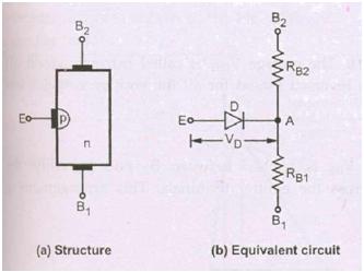
  • It is a three terminal device, having two layers. It consists of a slab of lightly doped n type silicon material. The two base contacts are attached to both the ends of this n type surface. These are denoted as B1 and B2 respectively.

  • A  p  type  material  is  used  to  form  a  p-n  junction  at  the  boundary  of  the aluminum rod and n type silicon slab. The third terminal called emitter (E) is  taken out from this p-type material.

  • The n-type is lightly doped while p type is heavily doped.

  • As  n type  is  lightly  doped,  it  provides  high  resistivity  and  p  type  as heavily doped; the symbolic representation of UJT is shown in the Fig.

  • The  emitter  is  shown  by  an  arrow  which  is  at  an  angle  to  the  vertical  line representation n type material.

  • This  arrow  indicates  the  direction  of  flow  of  conventional  current  when  the UJT is forward biased.

EQUIVALENT CIRCUIT OF UJT


The  internal  resistances  of  the  two  bases  are  represented  as  RB1  and  RB2  In  the actual  construction,  the  terminal  E  is  closer  to  B2  as  compared  to  B1.  Hence resistance RB1 is more than the resistance RB2. The p-n junction is represented by a normal diode with VD as the drop across it. When the emitter diode is not conducting     then the resistance between the two bases B1 and B2 is called interbase resistance   denoted as RBB.

Its value ranges between 4k and 12K.

Intrinsic Stand off Ratio:

Consider UJT as shown in the to which supply VBB is connected with IE=0  i.e. emitter diode is not conducting,

Then the voltage drop across RB1 can be obtained by using potential divider rule.


The typical range of   is from 0.5 to 0.8. The voltage VRB1 is called intrinsic stand off voltage  because  it  keeps  the  emitter  diode  reversed  biased  for  all  the  emitter voltages less than VRB1

PRINCIPLE OF OPERATION:

While operating an UJT, the supply VBB is applied between B1 and B2 whilethe   variable   emitter   voltage   VE   is   applied   across   the   emitter   terminals.   This arrangement is shown in the Fig


Let us see the effect of change in VE. The potential of A is decided by   and is equal to  VBB.

Case1: VE

As  long  as  VE  is  less  than  VA,  the  p-n  junction  is  reverse  biased.  Hence  emitter current IE will not flow. Thus UJT is said to be OFF.

Case 2 : VE> Vp

The diode drop VD is generally between 0.3 to 0.7 V. Hence we can write,

Vp = VA+VD=  VBB+ VD

When  V  becomes  equal  to  or  greater  than  Vp  the  p-n  junction  becomes  forward biased and current IE flows. The UJT is said to be ON.

UJT CHARACTERISTICS


The  graph  of  emitter  current  against  emitter  voltage  plotted  for a  particularvalue  of  VBB  is  called  the  characteristics  of  UJT.  For  a  particular  fixed  value  of  VBB such characteristics is shown in the Fig.


The characteristics can be divided into three main regions which are,

1. Cut off region:  The  emitter  voltage  VE  is  less than  Vp  and  the  p-n  junction  is reverse  biased.  A  small  amount  of  reverse  saturation  current  flows  through  the device,  which  is  negligibly  small  of  the  order of  µA.  This  condition  remains  till  the peak point.

2. Negative resistance region: When the emitter voltage VE becomes equal to Vp the  p-n  junction  becomes  forward  biased  and  IE  starts  flowing.  The  voltage  across the device decreases in this region, though the current through the device increases.   Hence the region is called negative resistance region. This decreases time resistance RB1.  This  region  is  stable  and  used  in  many  applications.  This region  continues  fill valley point.

3. Saturation region: Increase in IE further valley point current IV drives the device
in  the  saturation  region.  The  voltage  corresponding  to  valley  point  is  called  valley point voltage denoted as Vv. In this region, further decrease in voltage does not take   place.  The  characteristic  is  similar  to  that  of  a semiconductor  diode,  in  this  region. The  active  region  i.e.  negative  resistance  regions,  the  holes  which  are  large  in number on p-side, get injected into n-side. This causes increase in free electrons in the n-type slab. This increases the conductivity i.e. decreases the resistivity. Hence the  resistance  R  decreases  in  this  region.  As  the  VBB  increases,  the  potential  VP corresponding to peak point will increase.

Applications

  • The UJT is mainly used in the triggering of other devices such as SCR.

  • It is also used in the sawtooth wave generators and some timing circuits.

  • The  most  popular  application  of  UJT  is  as  a  relaxation  oscillator  to  obtain short pulses for triggering of SCRs.

DIAC


The  construction  of  a  diac  is  similar  to  an  open  base  “NPN”  transistor.  A simple block diagram is shown in Figure.

Diac Block Construction 


The  bidirectional  transistor-like structure  exhibits  a high-impedance  blocking state  up  to  a  voltage  Breakover  point  (VBO)  above  which  the  device  enters  a negative-resistance  region.  These  basic  diac  characteristics  produce  a  bidirectional pulsing  oscillator  in  a  resistor-capacitor  AC  circuit.  Since  the  diac  is  a  bidirectional device, it makes a good economical trigger for firing triacs in phase control circuits like light dimmers, motor speed controls, etc. Figure is a simplified AC circuit using a     diac and a triac in a phase control application.

Applications of DIAC

Some of the circuit applications of diac are

i) Light dimmer circuits

ii) Heat control circuits

iii) Universal motor speed control.

TRIAC

  • Two  thyristors  may be connected in inverse parallel,  but  at  moderate  powerlevels  the  two  antiparallel  thyristors  can  be  integrated  into  a  single  device structure, as shown.
  • This  device  commonly  known  as  Triac  (triode a.c.  switch)  is  represented  bythe circuit symbol shown.
  • Triac  is  the  word  derived  by  combining  the  capital  letters  from  the  wordsTRIode  &  a.c.  As  the  Triac  can  conduct  in  both  the  directions,  the  terms anode & cathode are not applicable to Triac.
  • Its three terminals are usually designated as main terminals, MT1, MT2 & gateG, as in a thyristor.
  • The  terminals  MT1is  the  reference  point  for  measurement  of  voltages  &currents  at  the  gate  terminal  &  at  the  terminal  MT2.  The  gate  is  near  to terminal MT1.
  • The V-I characteristics of a Triac is shown. This characteristic of the Triac arebased on the terminal MT1 as the reference point.

  • The first quadrant is the region wherein MT2 is positive with respect to MT1 &vice-versa for the third quadrant.
  • The  peak  voltage  applied  across  the  device  in  either  direction  must  be  lessthan the break over voltage in order to retain control of the gate.
  • A  gate  current  of  specified  amplitude  of  either  polarity  will  trigger  the Triacinto conduction in either quadrant, assuming that the device is in a blocking condition initially before the gate signal is applied.
  • The characteristics of a Triac are similar to those of SCR, both in blocking &conducting states, expect for the fact that SCR conducts only in the forward direction, whereas the Triac conducts I both directions.
  • Depending  upon  the  polarity  of  a  gate  pulse  &  biasing  conditions,  the  mainfour-layer structure that turns on by a regenerative process could be one of P1N1 P2N2, P1N1 P2N3, or P2N1 P1N4,


TRIGGERING MODES OF TRIAC

Triggering can be obtained from d.c., rectified a.c., or pulse sources such as
unijunction  transistors  &  switching  diodes  such  as  the  Diac,  silicon  bilateral  switch (SBS) & asymmetrical trigger switch.


1. MT2 positive, positive gate current (MODE 1)


When  the  gate  current  is  positive  with  respect  to  MT1  ,  gate  current  flows normally  from  the  gate  lead  to  the  terminal  MT1  through  the  P2  –  N2  junction  as shown. The  device  turns  on  in  the  conventional  manner  as  in  the  case  of  an  SCR. However, in the case of a Triac, the gate current requirement is higher for turn on at a  particular voltage.  Because  of  ohmic  contacts of  gate & MT1  terminals  on  the  P2- layer, some more gate current flows from the gate lead G to the main terminal MT1    through  the  semiconductor  P2  layer  without  passing through  the  P2N2 junction. The main  structure which  ultimately turns  on through  regenerative  action is  P1N1 P2N2.


The P2   layer is  flooded  with electrons  when the  gate current  flows  across  the P2N2 junction. These electrons diffuse to the  edge  of  the  junction J2, are collected by N1 layer. Therefore, the electrons build a space charge in the N1 region & more holes from P1 diffuse into N1 to neutralize the negative space charge. These holes arrive at    the junction J2. They produce a positive space charge in the P2 region which results
in more electrons being injected from N2 into P2. This results in positive regeneration & ultimately the structure P1N1 P2N2 conducts the external current.

2. MT2 positive, negative gate current (MODE 2)


A  cross  sectional  view  of  the  structure  is  shown.  When  the  terminal  MT2  is positive & gate terminal is negative with respect to terminal MT1, gate current flows through P2-N3 junction & this gate current IG forward biases the gate current P2-N3 of the auxiliary P1N1 P2N  3structure. As a result, Triac starts conducting through P1N1 P2N3 layers initially. With the conduction of P1N1 P2N3, the voltage drop across it falls but potential of layer between P2N3 rises towards the anode potential of MT2. As the right  hand  portion  of  P2  is  clamped  at  the  cathode  potential  of  MT1,  a  potential gradient  exists  across  layer  P2  from,  its  left  hand  region  begin  at  higher  potential than its right hand region. A current is thus established in layer P2 from left to right which  forward  biased  P2N2  junction  &  finally  the  main  structure  P1N1  P2N2,  may  be considered as a pilot SCR, while the structure OP1 N1 P2N2 may be regarded as the main SCR, both begin built in one common structure. The anode current of the pilot
SCR serves as the gate current for the main SCR. As compared with turn on process,
the  device  with  MT2 positive but  gate current negative is less sensitive & therefore
more gate current is required.

3. MT2 negative, positive gate current (MODE 3)


When terminal  MT2 is negative & terminal MT1 is  positive,  the device  can  be turned on  by  applying a  positive  voltage  between  the  gate &  terminal  MT1. In  this mode, the device operates in the third quadrant when it is triggered into conduction.    The turn on is initiated by remote gate control. The main structure that leads to turn on is P2N1 P1N4 with N2 acting as a remote gate as shown. The external gate current IG forward biases P2N2

SILICON CONTROLLED RECTIFIER


  • It  is  a  four  layered  PNPN  device  and  is  a  prominent  member  of  thyristorfamily.   It consists of   three diodes   connected   back   to   back   with   gate connection or two complementary transistor connected back to back.
  • It  is  widely  used  as  switching  device  in  power  control  applications.  It  canswitch ON for variable length of time and delivers selected amount of power to load.
  • It  can  control  loads,  by  switching  the  current  OFF  and  ON  up  to  manythousand  times  a  second.  Hence  it  possess  advantage  of  RHEOSTAT  and  a switch with none of their disadvantages
Construction

As  shown  in  figure  1  it  is  a  four  layered  three terminal  device, layers  being
alternately  P-type  and  N-type  silicon.  Junctions  are  marked  J1,  J2,  J3  whereas terminals are anode (A), cathode
(C) and gate
(G). The gate terminal is connected to inner P-type layer and it controls the firing or switching of 5CR.

Biasing


The  biasing of  SCR is  shown  in  figure  
1(a).  The  junction  J1  and  J3  become
forward biased while J2 is reverse biased. In figure 1 polarity is reversed. It is seen that now junction J1 and J3 become reverse biased and only J2 is forward biased.

Operation of SCR

  • In  SCR  a  load  is  connected  in  series  with  anode  and  is  kept  at  positivepotential  with  respect  to  cathode  when  the  gate  is  open  i.e.,  no  voltage  is applied at the gate.
  • Under this condition, junctions J1 and J3 are for ward biased and junction J2is reverse biased. Due to this, no current flows through RL and hence the 8CR is cutoff.
  • However when the anode voltage is increased gradually to breakover voltage,then  breakdown  occurs  at  junction  J  due  to  this  charge  carriers  are  able  to flow from cathode to anode easily, hence SCR starts conducting and is said tobe in ON state.
  • The SCR  offers  very  small forward  resistance so that  it  allows infinitely highcurrent.  The  current  flowing  through  the  8CR  is  limited  only  by  the  anode voltage and external resistance.
  • If  the  battery  connections  of  the  applied  voltage  are  reversed  as  shown  infigure 2 the junction J1 and J3 are reverse biased. J2 is forward biased.
  • If  the  applied  reverse voltage is  small  the  SCR is  OFF  and  hence no  currentflows through the device.
  • If the reverse voltage is increased to reverse breakdown voltage, the junctionJ1 and J3 will breakdown due to avalanche effect. This causes current to flow through the SCR.
  • From the above discussion we conclude that the SCR can be used to conduct only in forward direction. Therefore SCR is called as “unidirectional device”.
Vl Characteristics of SCR

The  “forward characteristics”   of SCR may be obtained using the figure 3.

The volt-ampere characteristics of a SCR for IG = 0 is shown in figure 3.


  • As the applied anode to cathode voltage is increased above zero, very smallcurrent flows through the device, under this condition the 5CR is off. It will be continued  until;  the  applied  voltage  reaches  the  forward  Breakover  voltage (point A).
  • if  the  anode-cathode  (applied)  voltage  exceeds  the  Breakover  voltage  itconducts heavily the SCR turns ON  and  anode to  cathode voltage decreases quickly  to  a  point  B  because,  under  this  condition  the  5CR  offers  very  low resistance hence it drops very low voltage across it.
  • At this stage the 5CR allows more current to low through it. The amplitude ofthe   current   is   depending   upon   the   supply   voltage   and   load   resistance connected in the circuit.
  • The current corresponding to the point ‘B’ is called the “holding current (IH)”It can be defined as the minimum value of anode current required to keep the     SCR  in  ON  State.  If  the  5CR  falls  below  this  holding  current  the  SCR  turns OFF.
  • If the value of the gate current I is increased above zero, (‘G > O) the SCRturns ON even at lower Breakover voltage as shown in figure 3(b).
  • The region lying between the points OA is called forward blocking region. Inthis  region  5CR  is  OFF’.  The  region  lying  between  the  points  BC  is  called forward conduction region. In this region SCR is ON.
  • Once  the  SCR  is  switched  ON  then  the  gate  looses  all  the  control.  So  SOBcannot  be  turned  OFF  by  varying  the  gate  voltage.  It  is  possible  only  by reducing the applied voltage.
To obtain the “reverse characteristics”the following points are followed.

1.In  this  case  the  SCR  is  reverse  biased,  if  the  applied  reverse  voltage  is increased  above  zero,  hence  a  very  small  current  flows  through  the  SCR.

 Under  this  condition  the  SCR  is  OFF,  it  continues  till  the  applied  reverse voltage reaches breakdown voltage.

2.As the applied reverse voltage is increased above the breakdown voltage, the avalanche  breakdown  occurs  hence  5CR  starts  conducting  in  the  reverse direction. It is shown in curve DE. Suppose the applied voltage is increased to   a very high value, the device may get damaged.

SCR rating

The SCR rating are defined as follows

1)  “Forward  Breakover  voltage”:It   is   the   voltage   at   which   the   5CR  is switched  from  its  OFF  position  to  ON  position.  Its:  values  are maximum  for zero gate current, its values lie in the range of 50 to l200volts

2)  “Holding  current”:  it  is  the  minimum  value  of  anode  current  required  to keep the SCR in ON position.

3)   “Gate  triggering  current”:    It  is  the  value  of  anode  current  necessary  to switch  5CR from  OFF to  ON  position under specified condition. It  is  typically   about 4OmA.

4)   “Average forward current”:   It is the maximum value of anode current at which the 5CR can handle in its ON position. Its value lies in the range of 1 to 1800Amps.

5)   “Reverse breakdown voltage”:   It is the value of reverse voltage between cathode to anode at which the avalanche breakdown occurs.

6)  “Turn ON time – TON”: It can be defined as, the time required to switch it from OFF to ON state when triggering signal is applied. TON decreases if the trigger voltage is increased; TON is increases when anode current increases.

7)   “Turn OFF Time – TOFF”: It is the time required to switch it  from ON to OFF  state  by  dropping  anode  voltage.  TOFF  is  small  if  anode  voltage  in reverse direction and increases with temperature and anode current.

8)  “Gate  Recovery  time”:    It  is  the  time  required  for  which  anode  voltage  is reduced to VH to turn OFF SCR.

Basic Operation of an SCR

The operation of a PNPN device can best be visualized as a specially coupled
pair of transistors as shown in Figure


The  connections  between the  two transistors  are  such that  regenerative  action  can occur when a proper gate signal is applied to the base of the NPN transistor. Normal leakage  current  is  so  low  that  the  combined  hFE  of  the  specially  coupled  two- transistor  feedback  amplifier  is  less  than  unity,  thus  keeping  the  circuit  in  an  off- state  condition.  A  momentary  positive  pulse  applied  to  the  gate  will  bias  the  NPN transistor into conduction  which, in turn,  biases  the  PNP transistor into conduction.    The  effective  hFE  momentarily  becomes  greater  than  unity  so  that  the  specially coupled  transistors  saturate.  Once  saturated,  current  through  the  transistors  is enough to keep the combined hFE greater than unity. The circuit will remain “on” until    it  is  “turned  off”  by  reducing  the  anode-to-cathode  current  (IT)  such  that  the combined  hFE  is  less  than  unity  and  regeneration  ceases;  this  threshold  anode current is the holding current of the SCR.

Electrical Characteristic Curves of Thyristors V-I Characteristics of SCR Device


Methods of Switching on Thyristors There are three general ways to switch thyristors to on-state condition:

  • Application of Gate Signal
  • Static dv/dt Turn-On
  • Voltage Breakover Turn-On
Listed below is a brief description of each method.

Application Of Gate Signal

For an SCR (unilateral device), this signal must be positive with respect to the cathode polarity. A triac (bilateral device) can be turned on with gate signal of either polarity;  however,  different  polarities  have  different  requirements  of  IGT  and  VGT which must be satisfied. Since a diac does not have a gate, this method of turn-on is     not applicable to diacs; in fact, the single major application of diacs is to switch-on   triacs.

Static dv/dt Turn-On

Comes  from  a  fast  rising  voltage  applied  across  the  anode  and  cathode terminals of an SCR or the main terminals of a triac. Due to the nature of thyristor construction,  a  small  junction  capacitor  is  formed  across  each  PN  junction.  Figure 14.14  shows  how  typical  internal  capacitors  are  linked  in  gated  thyristors.  When voltage  is  impressed  suddenly  across  a  PN  junction,  a  charging  current  will  flow which is equal to:

i = C (dv/dt)

When   c   (dv/dt)   becomes   greater   or  equal  to  thyristor  IGT,  the thyristor  switches  on.  Normally,  this  type  of  turn  on  does  not  damage  or  hurt the device providing the surge current is limited. Generally, thyristor application circuits are designed with static dv/dt snubber networks if fast rising voltages are
anticipated.

Voltage Breakover Turn-On

Is the method used to switch on diacs. However, exceeding voltage break over of SCRs and triacs is definitely not recommended as a turn-on method. In the case of   SCRs  and  triacs,  the  leakage  current  increases  until  it  exceeds  the  gate  current required  to  turn-on  these  gated  thyristors  in  a  small  localized  point.  When  turn-on occurs by this method, there is localized heating in a small area which may melt the    silicon  or  damage  the  device  if  di/dt  of  the  increasing  current  is  not  sufficiently limited.  Diacs  used  in  typical  phase  control  circuits  are  basically  protected  against excessive  current  at  breakover  as  long  as  the  firing  capacitor  is  not  excessively large. When diacs are used in a zener function, current limiting is necessary.

Labels

PROJECTS 8086 PIN CONFIGURATION 80X86 PROCESSORS TRANSDUCERS 8086 – ARCHITECTURE Hall-Effect Transducers INTEL 8085 OPTICAL MATERIALS BIPOLAR TRANSISTORS INTEL 8255 Optoelectronic Devices Thermistors thevenin's theorem MAXIMUM MODE CONFIGURATION OF 8086 SYSTEM ASSEMBLY LANGUAGE PROGRAMME OF 80X86 PROCESSORS POWER PLANT ENGINEERING PRIME MOVERS 8279 with 8085 MINIMUM MODE CONFIGURATION OF 8086 SYSTEM MISCELLANEOUS DEVICES MODERN ENGINEERING MATERIALS 8085 Processor- Q and A-1 BASIC CONCEPTS OF FLUID MECHANICS OSCILLATORS 8085 Processor- Q and A-2 Features of 8086 PUMPS AND TURBINES 8031/8051 MICROCONTROLLER Chemfet Transducers DIODES FIRST LAW OF THERMODYNAMICS METHOD OF STATEMENTS 8279 with 8086 HIGH VOLTAGE ENGINEERING OVERVOLATGES AND INSULATION COORDINATION Thermocouples 8251A to 8086 ARCHITECTURE OF 8031/8051 Angle-Beam Transducers DATA TRANSFER INSTRUCTIONS IN 8051/8031 INSTRUCTION SET FOR 8051/8031 INTEL 8279 KEYBOARD AND DISPLAY INTERFACES USING 8279 LOGICAL INSTRUCTIONS FOR 8051/8031 Photonic Transducers TECHNOLOGICAL TIPS THREE POINT STARTER 8257 with 8085 ARITHMETIC INSTRUCTIONS IN 8051/8031 LIGHTNING PHENOMENA Photoelectric Detectors Physical Strain Gage Transducers 8259 PROCESSOR APPLICATIONS OF HALL EFFECT BRANCHING INSTRUCTIONS FOR 8051/8031 CPU OF 8031/8051 Capacitive Transducers DECODER Electromagnetic Transducer Hall voltage INTEL 8051 MICROCONTROLLER INTEL 8251A Insulation Resistance Test PINS AND SIGNALS OF 8031/8051 Physical Transducers Resistive Transducer STARTERS Thermocouple Vacuum Gages USART-INTEL 8251A APPLICATIONs OF 8085 MICROPROCESSOR CAPACITANCE Data Transfer Instructions In 8086 Processors EARTH FAULT RELAY ELECTRIC MOTORS ELECTRICAL AND ELECTRONIC INSTRUMENTS ELECTRICAL BREAKDOWN IN GASES FIELD EFFECT TRANSISTOR (FET) INTEL 8257 IONIZATION AND DECAY PROCESSES Inductive Transducers Microprocessor and Microcontroller OVER CURRENT RELAY OVER CURRENT RELAY TESTING METHODS PhotoConductive Detectors PhotoVoltaic Detectors Registers Of 8051/8031 Microcontroller Testing Methods ADC INTERFACE AMPLIFIERS APPLICATIONS OF 8259 EARTH ELECTRODE RESISTANCE MEASUREMENT TESTING METHODS EARTH FAULT RELAY TESTING METHODS Electricity Ferrodynamic Wattmeter Fiber-Optic Transducers IC TESTER IC TESTER part-2 INTERRUPTS Intravascular imaging transducer LIGHTNING ARRESTERS MEASUREMENT SYSTEM Mechanical imaging transducers Mesh Current-2 Millman's Theorem NEGATIVE FEEDBACK Norton's Polarity Test Potentiometric transducers Ratio Test SERIAL DATA COMMUNICATION SFR OF 8051/8031 SOLIDS AND LIQUIDS Speed Control System 8085 Stepper Motor Control System Winding Resistance Test 20 MVA 6-digits 6-digits 7-segment LEDs 7-segment A-to-D A/D ADC ADVANTAGES OF CORONA ALTERNATOR BY POTIER & ASA METHOD ANALOG TO DIGITAL CONVERTER AUXILIARY TRANSFORMER AUXILIARY TRANSFORMER TESTING AUXILIARY TRANSFORMER TESTING METHODS Analog Devices A–D BERNOULLI’S PRINCIPLE BUS BAR BUS BAR TESTING Basic measuring circuits Bernoulli's Equation Bit Manipulation Instruction Buchholz relay test CORONA POWER LOSS CURRENT TRANSFORMER CURRENT TRANSFORMER TESTING Contact resistance test Current to voltage converter DAC INTERFACE DESCRIBE MULTIPLY-EXCITED Digital Storage Oscilloscope Display Driver Circuit E PROMER ELPLUS NT-111 EPROM AND STATIC RAM EXCITED MAGNETIC FIELD Electrical Machines II- Exp NO.1 Energy Meters FACTORS AFFECTING CORONA FLIP FLOPS Fluid Dynamics and Bernoulli's Equation Fluorescence Chemical Transducers Foil Strain Gages HALL EFFECT HIGH VOLTAGE ENGG HV test HYSTERESIS MOTOR Hall co-efficient Hall voltage and Hall Co-efficient High Voltage Insulator Coating Hot-wire anemometer How to Read a Capacitor? IC TESTER part-1 INSTRUMENT TRANSFORMERS Importance of Hall Effect Insulation resistance check Insulator Coating Knee point Test LEDs LEDs Display Driver LEDs Display Driver Circuit LM35 LOGIC CONTROLLER LPT LPT PORT LPT PORT EXPANDER LPT PORT LPT PORT EXTENDER Life Gone? MAGNETIC FIELD MAGNETIC FIELD SYSTEMS METHOD OF STATEMENT FOR TRANSFORMER STABILITY TEST METHODS OF REDUCING CORONA EFFECT MULTIPLY-EXCITED MULTIPLY-EXCITED MAGNETIC FIELD SYSTEMS Mesh Current Mesh Current-1 Moving Iron Instruments Multiplexing Network Theorems Node Voltage Method On-No Load And On Load Condition PLC PORT EXTENDER POTIER & ASA METHOD POWER TRANSFORMER POWER TRANSFORMER TESTING POWER TRANSFORMER TESTING METHODS PROGRAMMABLE LOGIC PROGRAMMABLE LOGIC CONTROLLER Parallel Port EXPANDER Paschen's law Piezoelectric Wave-Propagation Transducers Potential Transformer RADIO INTERFERENCE RECTIFIERS REGULATION OF ALTERNATOR REGULATION OF THREE PHASE ALTERNATOR Read a Capacitor SINGLY-EXCITED SOLIDS AND LIQUIDS Classical gas laws Secondary effects Semiconductor strain gages Speaker Driver Strain Gages Streamer theory Superposition Superposition theorem Swinburne’s Test TMOD TRANSFORMER TESTING METHODS Tape Recorder Three-Phase Wattmeter Transformer Tap Changer Transformer Testing Vector group test Virus Activity Voltage Insulator Coating Voltage To Frequency Converter Voltage to current converter What is analog-to-digital conversion Windows work for Nokia capacitor labels excitation current test magnetic balance voltage to frequency converter wiki electronic frequency converter testing voltage with a multimeter 50 hz voltages voltmeter

Search More Posts

Followers