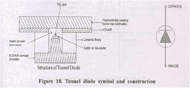
- The tunnel diode is a thin junction diode; under forward bias condition itexhibits negative resistance. This makes the tunnel diode Useful foroscillations or amplification.
- In conventional PN diode is doped to have impurity atoms in theconcentration of 1 part in 108. Then the width of the depletion layer is of the order of a micron i.e., 5 micron.
- But in tunnel diode the impurity concentration is greatly increased to 1 part in103 then the depletion layer width reduces to about 100A thus device characteristics get completely changed.
- This diode utilizes the phenomenon called tunneling and hence the diode isreferred as tunnel diode.
- The width of the junction barrier varies inversely as the square root of theimpurity concentration (i.e) if the concentration. of impurity atom is greatly increased, the barrier width ‘W’ reduces.
- A particle must have an energy atleast equal to the height of the potentialbarrier in order to cross over the junction. However if the barrier is extremely thin, then instead of crossing over the junction barrier the electron may penetrate through the barrier.
- This behavior exhibited by the electron to the applied potential is called“tunnelling” and hence the diode is called as tunnel diode.
- Thus a tunnel diode is a high conductivity two terminal PN Junction diodedoped heavily about 1000 times higher than a conventional junction diode.
VI Characteristics:
- The heavily doped tunnel diode results in a thin depletion layer so as topermit tunnelling to occur. The VI characteristic of a typical germanium tunnel diode is shown in the figure 19.
- It is seen at first the current rise sharply as voltage is applied and reaches thepeak current Ip point (A).
- As the forward bias is increased above this point (A) the forward currentdrops and continues to drop until! a point B is reached. This point is the Valley voltage or valley current (Iv)
- After the valley point is reached further increase in input voltage increasesthe current very rapidly as PN junction diode.
- The tunnel diode exhibits negative resistance characteristics seen betweenthe peak current IP and minimum value IV and it is called valley current.
- The peak current IP depend on the impurity. Tunnel diodes with 1 to 100 mA,are commonly used in computer applications.
Equivalent circuit of Tunnel diode
where,
c = junction capacitance = 1 to 10 PF -RN = negative resistance of diode
Ls = inductance due to terminal leads.
Advantage
1. Low Cost
2. Simplicity of construction
3. High Speed Operation
4. Low Temperature senstivity, low noise and low power
5. Environmental immunity
Disadvantage
1. Low output voltage swing
2. Since it is two terminal device there is no isolation between input and output.
Applications
1. Tunnel diode amplifiers may be used throughout the micro-wave range as moderate to low-noise pre amplifiers in all kinds of receivers.
2. Tunnel diode are used as mixers
3. Being high-speed devices, tunnel diode also lend them selves to high speed switching and logic operations as flip flop and gate.
4. Finally they are used as low power oscillator upto about l000Hz,because of their simplicity, frequency stability and immunity to radiation.


Prof. Prem raj Pushpakaran writes -- 2025 marks the birth centenary year of Leo Esaki, and let us celebrate the occasion!!! https://worldarchitecture.org/profiles/gfhvm/prof-prem-raj-pushpakaran-profile-page.html
ReplyDelete